

Hello everybody!
Worn-out NAND Flash chips are a common issue when we are speaking about data recovery from USB Flash devices. Nowadays chips may have low quality even from the factory. Your pendrive may die less than in a month because of that. Unfortunately, such a tendency can also be seen when we are talking about other devices in which NAND chips can be used, for example, SSDs, mobile phones, and even modern cars!
Tesla vehicles built between 2012 and 2018 use an infotainment system powered by Nvidia’s Tegra 3 system-on-chips that include 8GB of eMMC NAND storage. The trouble is that these Flash chips are wearing out, having hit their program-erase cycle limits, and are unable to store data reliably, causing glitches in operation. Around 160 000 cars were produced with such eMMC storage inside and may be impacted by this problem. The storage controllers can no longer find good working NAND blocks to use and thus fail. Once the storage is worn out, it can have an impact on some of the car’s features like the touchscreen, rearview camera, defogging system and so on. In the worst of circumstances, it can even affect such vital options for Tesla cars as driving on Autopilot.
Tesla is already aware of these problems and has attempted to remedy the problem with some updates that reduced the number of logs being written, improved the error correction and storage strategies. Also, in May 2020, Tesla began producing spares that now use a 64GB Micron eMMC instead of 8GB eMMCs from Hynix.
But the main question is still there. What to do if you need to find and save some system files like keys and certificates?
Let’s check two real cases from such cars.
The first chip is SM controller, ADD79491 6044ADD7 memory, part size = 4096Mb, page size = 8832 bytes, block size = 2048 pages. In this case, the chip has two banks, but you can get chips with only one bank as well. We need to find the key file and the certificate file with names car.key and car.crt
To do that, we need to perform some preparation steps.
First of all, you need to read the dump from this chip. You need to find the pinout scheme.
After the dump has been successfully read, we begin with changing the block size.
Step 1. Because of the very large size of this drive, the first step is to change the block size to 4096 pages in the task. You can do it like this:

This action is necessary to apply XORs of this size. At a certain stage, you will need to return the original value of the block size equalling 256, but we will return to it later.
Step 2. Since we have a case with two banks, we ended up with a task with two dumps. The difference from one banking case is only in one “Join by Block/Pages” less.
So, the main problem with two banks is that there are XORs for each bank. You can see them in the XOR list at the top.

The name of the XOR contains information about the Chip Enable part and operation that would be performed (data decryption of the ECC area for error correction or data decryption of the Data Area for image assembly). In case of a single bank chip, XOR for CE1 is not needed.
Step 3. These are the typical preparation steps for such cases:
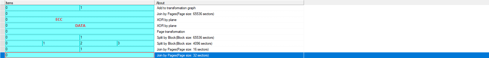
XORs in this case are used for some virtual plans the size of which we have set by changing the size of the chip’s block on the chip node. This little trick eliminates the need to correct and re-read the dumps in different graphs, that is, on the third line of the graph, we define the ECC, make the correction and re-read the invalid sectors. The fourth line of the graph is again XOR, but this is XOR for data and it is not self-sufficient, that’s why it is important to apply it after XOR for ECC. This XOR changing looks very similar to AU cases when we need to choose XOR for ECC first and then for the Block Number.
This is how page design should look like:
Page size: 16 sectors 8832
Sector size 544
Structure*
32-512; 0-32;
544-512; 0-32;
1126-512; 0-32;
1638-512; 0-32;
2220-512; 0-32;
2732-512; 0-32;
3314-512; 0-32;
3826-512; 0-32;
4408-512; 0-32;
4920-512; 0-32;
5502-512; 0-32;
6014-512; 0-32;
6596-512; 0-32;
7108-512; 0-32;
7690-512; 0-32;
8202-512; 0-32;
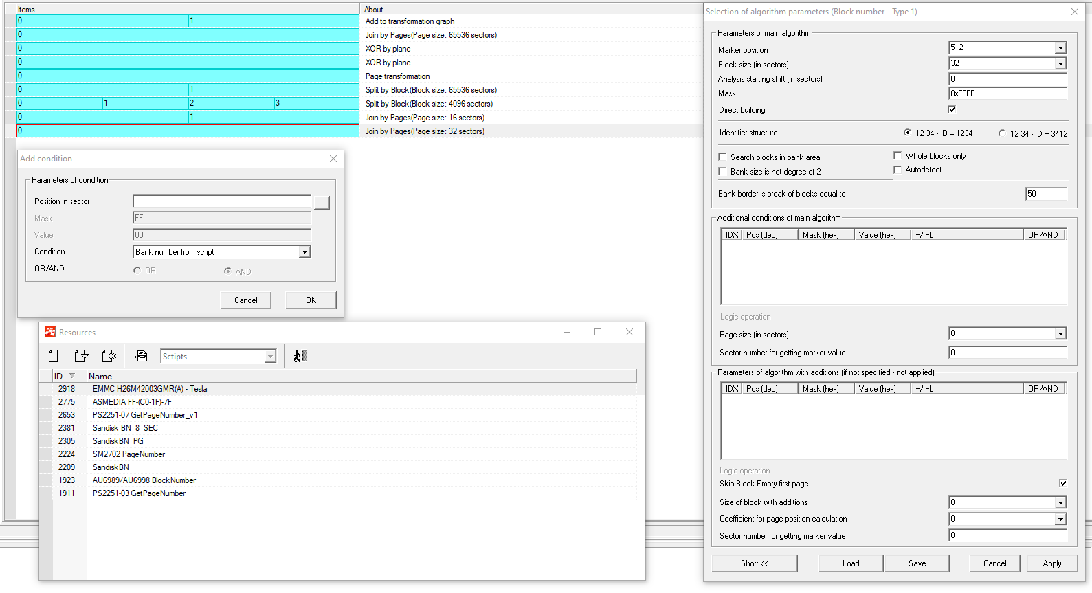
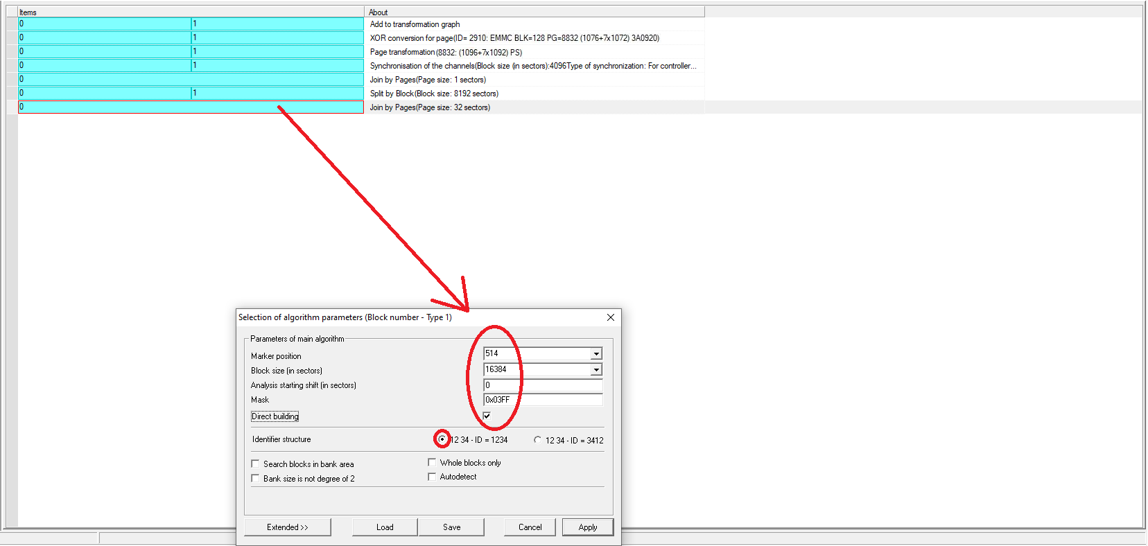
This is a very important step! Аfter all the transformations have been added, we return to step 1 of our actions and return the initial block size of 256 pages in the parameters.
After all the transformations have been completed, ECC has worked and the dumps have been re-read as much as possible, you can start building the image. The image is assembled using a special script. Please make sure that all the parameters are the same as in the picture.
In case of big problems with ECC you can use GREP search for car.crt using the pattern @4\x2D\x42\x45\x47\x49\x4E\x20\x43\x45\x52\x54 and for car.key @4\x2D\x42\x45\x47\x49\x4E\x20\x52\x53\x41\x20. Both types of files have a byte sequence 2D2D2D2D2D0A at the end of the files which can be used to determine the exact size of the file.
The second case is PS8032 controller or similar, 1×2 ADD794DA 74C30000 memory, part size = 4096Mb, page size = 8832 bytes, block size = 256 pages, dual-channel memory, which indicates the presence of two independent sets of IO0-7 lines.
In general, the second task is pretty similar to the case above but has some exceptions.
1. ECC on the first line of the graph should be defined like this:
– 0 [1076]
– 1076 [1072]
– 2148 [1072]
– 3220 [1072]
– 4292 [1072]
– 5364 [1072]
– 6436 [1072]
– 7508 [1072]
2. A typical set of transformations and assembly parameters should look like that:
Otherwise, the methods and problems are the same as in the first case of this article. The main problem is the quality of the dumps. The chips are usually worn out. As a result, it is easier to do all the transformations firstly, then find the necessary car.key and car.crt files by searching for GREP, and focus on re-reading the pages with these files. Please remember that the channels are different and the dumps are combined through the sector. That’s why you can re-read only on the first line of the graph, but save the files on the last one. For more convenient re-reading, you can slightly change the order of transformations to the following one:

If you have questions regarding your data recovery cases, you’re welcome to address them to the ACE Lab Technical Support Department.


Amazing Great job Ace lab…
Great job… But how to work in PC3k Flash with eMMC chips? 🙂 PC3k Flash can work with NAND flash chips, without microcontroller. But in this case TESLA uses eMMC chip. How to got ACELABboys data from damaged eMMC? 🙂 If you want to read NAND flash part from eMMC, you need find and use NAND flash PINs… What did you use? PC3k Mobile?
This feature (datarecovery from damaged eMMC) can ofer RUSOLUT eMMC, but ACELAB y/n?…
It will be new feature, new product of ACELAB? 🙂
Thank you
Hello Radovan,
We used a MultiBoard adapter to wire the eMMC and read the internal NAND core. You are right – this approach requires a layout. Lucky for us, we have a few of them 🙂
Unfortunately this approach of eMMC NAND Core reading isn’t effective for most of modern cases, because all more or less modern devices are using encryption. But for some old cases without encryption it works not so bad. We are still thinking about the possibility of developing a more user-friendly solution for such cases. Current article is just a good example of our research.