


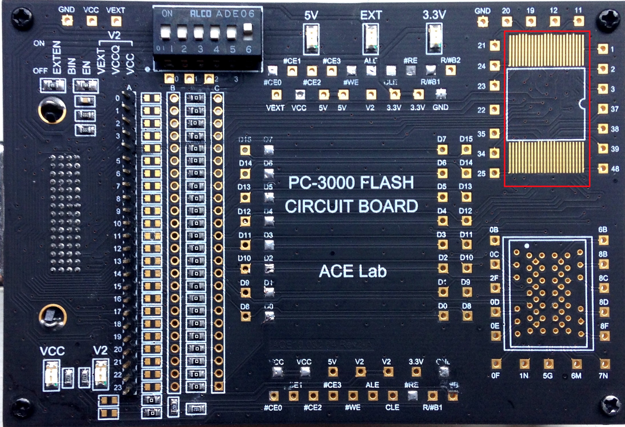
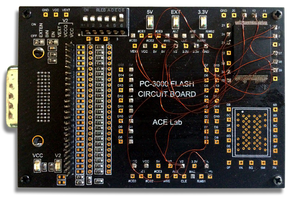
PC-3000 Circuit Board adapter is a really good and useful thing. First of all with the help of this adapter you can read the data from monolithic devices like mSD, SD, xD, MS and UFD. But at the same time, Circuit board works great in case if for some reason, we need to read data from common chips like TSOP-48, TSSOP-48 (short package) or BGA-52 with physical damages of pin legs.
Lets imagine that during chip unsoldering you damaged several legs of TSOP-48 memory, and you are not able to put it inside PC-3000 Flash reader. What should you do in this case? Of course you can try to repair this legs, make a serious job under microscope and restore the functionality of damaged legs. But this process will be very complicated, and during next chip installation into Flash reader socket, you can damaged them again.
That’s why the best decision in this case will be TSOP-48 chip soldering on Circuit Board adapter.
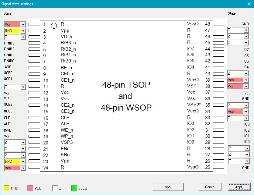
If you will look on it, you will see that current adapter has two installation set for BGA-52 and TSOP-48 chips.
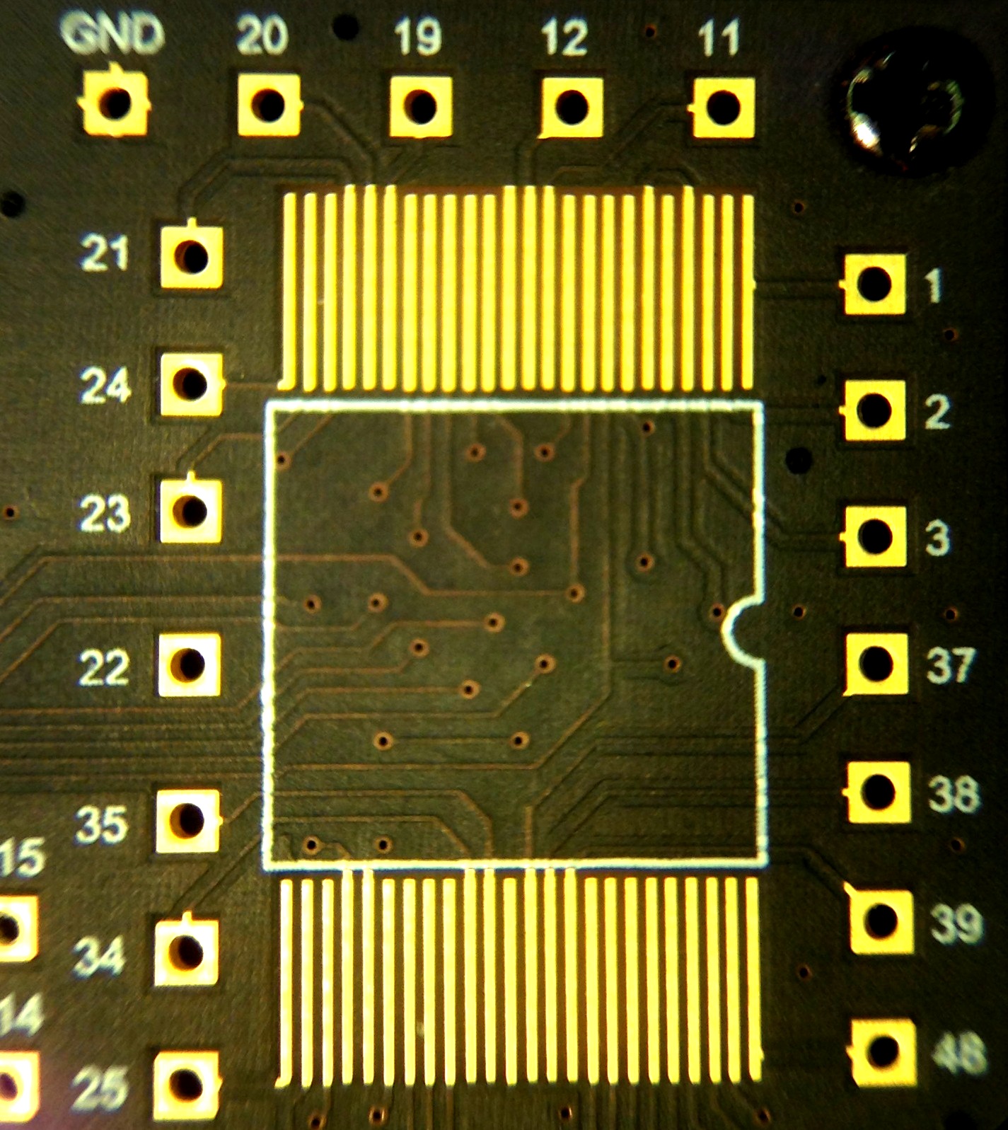
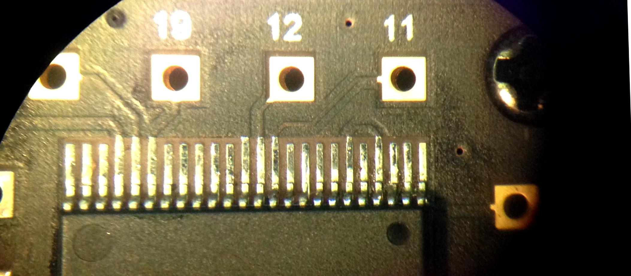
We are going to use TSOP-48. On Circuit board, some pins which are using for power supply or for additional power supply are not connected (Pins number: 1, 2, 3, 11, 12, 19, 20, 21, 22, 23, 24, 25, 34, 35, 37, 38, 39, 49).
First of all – we need to drop some liquid flux on the contacts for better soldering.
Than – necessary to put a layer of soldering tin at the place where we drop flux.

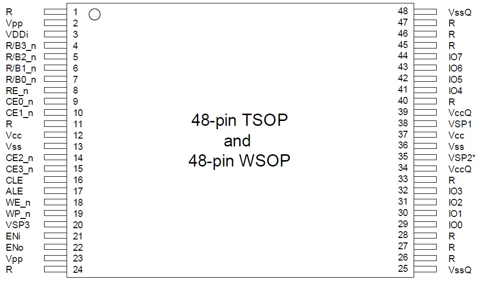
After that – we should start to solder our damaged TSOP-48 memory chip. Don’t forget that the KEY of memory chip should be situated near the pin number 1.
All legs are very small, that’s why we recommend to use microscope. When soldering will be finished, don’t forget to check all TSOP legs – they should not be able to move! All of them must be strongly fixed and soldered well. In case if some of the contacts are damaged, you can try to use small copper wires for easy chip leg repairing and soldering a wire from chip pin (leg) to compatible contact on Circuit Board.
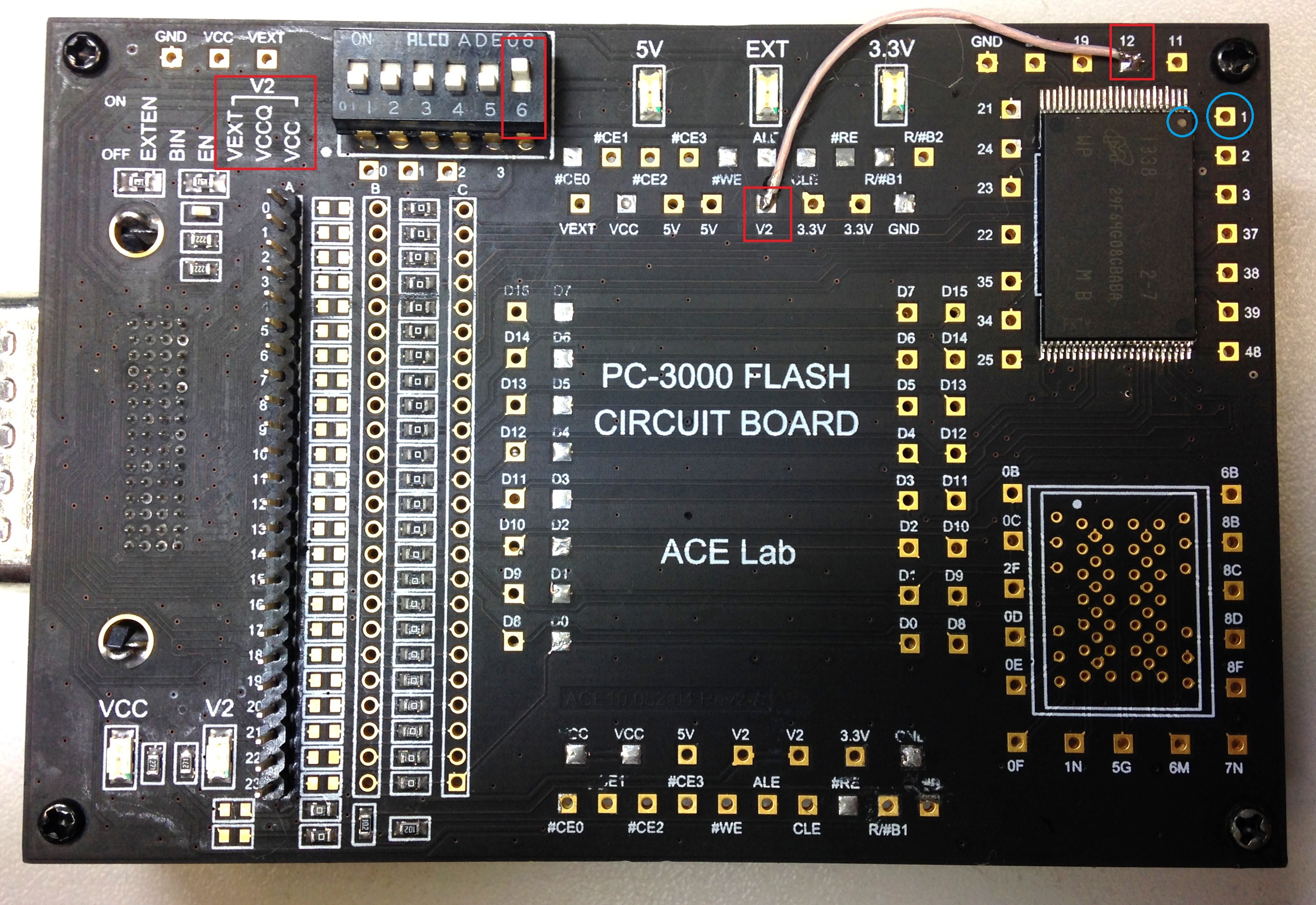
After that, we need to solder a wire from contact number 12 to V2 pin, which is used for Voltage Current Control from adapter. Without this wire, your soldered chip will not be power supplied!
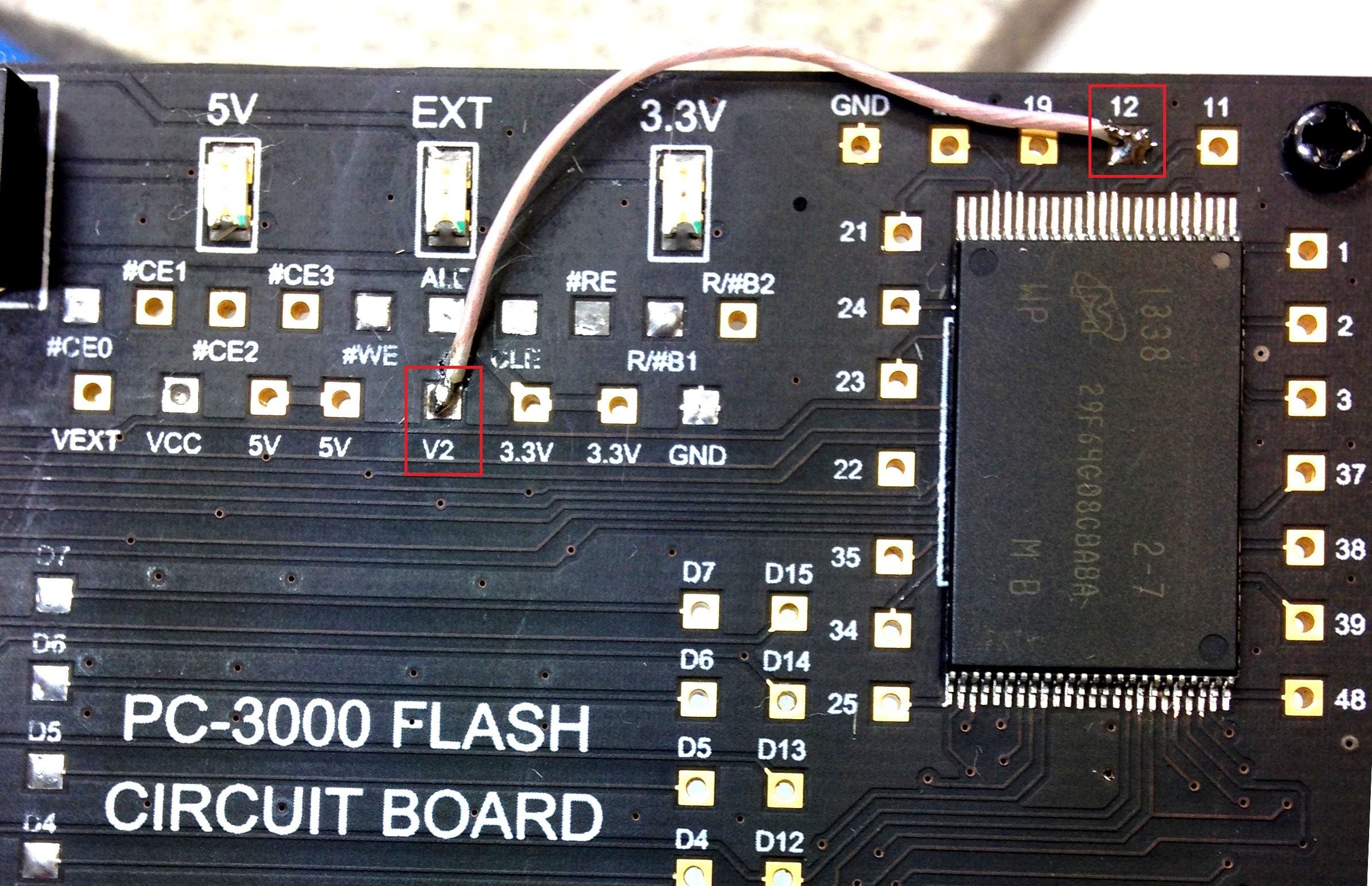
All triggers must be turned off except trigger number 6 (VCC from reader). In case if you want to use extended power supply adapter, you should configure triggers for external supply (see description in manual doc.).
The last step – don’t forget to use alcohol for board cleaning! We should remove all signs of flux from PCB and clean it!
Here it is! Final result. Now, we are ready to get dump from our TSOP-48 memory chip!
Such memory chip have a pimap #8 reading scheme. This is an old scheme with 1 power supply channel for all additional contacts of power supply on the chip. All modern chips have an special features like a Read Retry, Voltage control e.t.c. as result not enough to solder only one wire for power supply and we should to solder a separated wires for different power supply pins of memory chip.
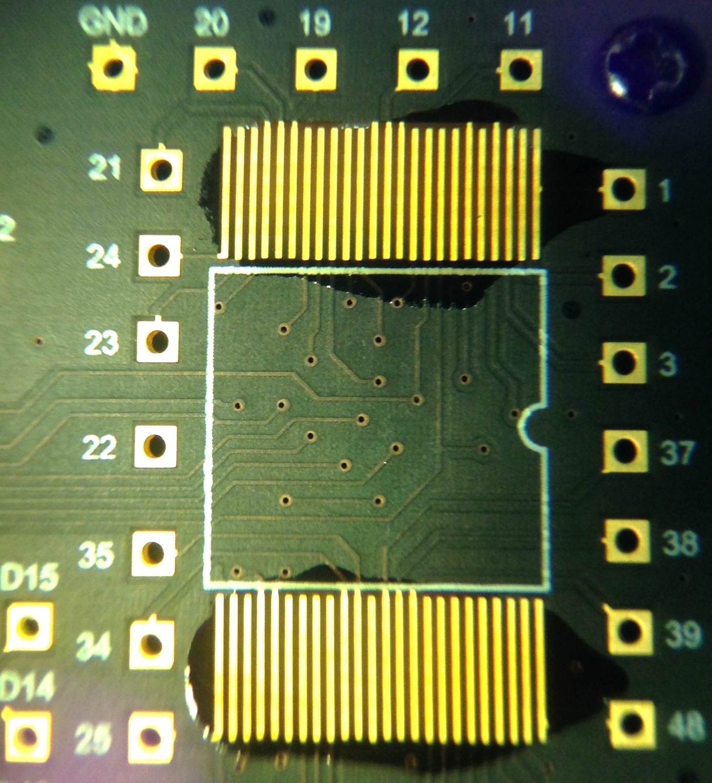
Here is a photo of soldered TSOP-48 chip by pinmap #9 reading scheme:
If solder memory chip to the Circuit board adapter by wrong pinmap reading scheme then possible following problems:
- Impossible to get a Chip ID (with out any error messages in log report)
- Shorting problem with such error message in log:
PWR ON Error on channel VCC. Overcurrent detected!
Current Limit: 200 mA
- Other problems with the power supply


When the “Circuit Board adapter” will be able to buy? And from how much? 🙂
You should ask our sales department. But as I know – already available for purchase 😉
What is the thickness of the wires used for the ponmap ? How thick they must be for electricity to power up the chip?
Usually it’s 0.2mm copper wires.