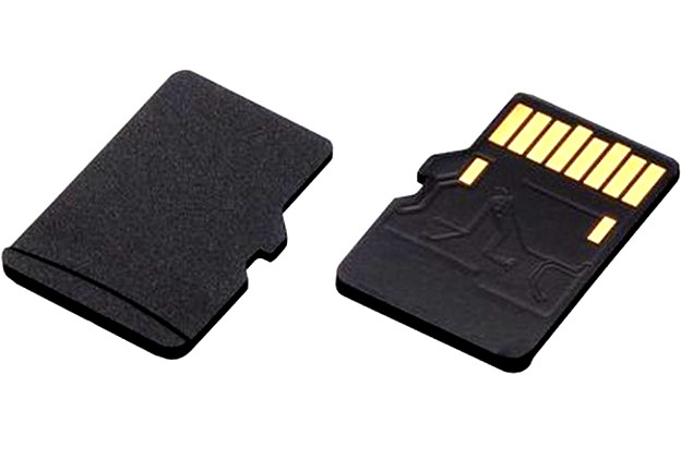
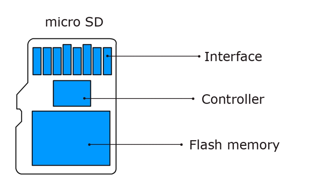
Nowadays a lot of modern NAND flash devices use a new type of architecture, where the interface, the controller and memory chips are integrated into one common ceramic layer. We call it Monolithic structure.
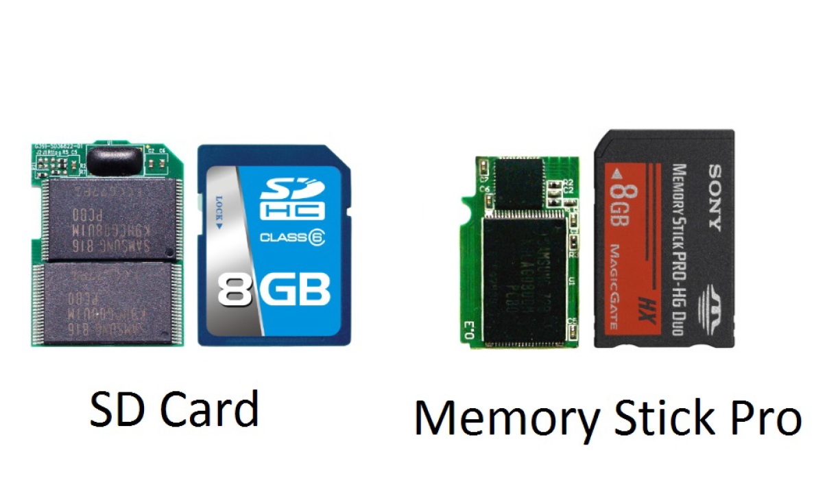
Until recently, all memory cards like SD, Sony MemoryStick, MMC and others, contained a very simple “classic” structure with separated parts – a controller, a PCB and a NAND memory chip in the TSOP-48 or LGA-52 package. In such cases, the full process of recovery was very simple – we just unsoldered the memory chip, read it in PC-3000 Flash, and made the same preparation as with common USB Flash drives.
But what should we do if our Memory Card, or UFD device is based on monolithic architecture? How can we get access to a NAND memory chip and read data from it?
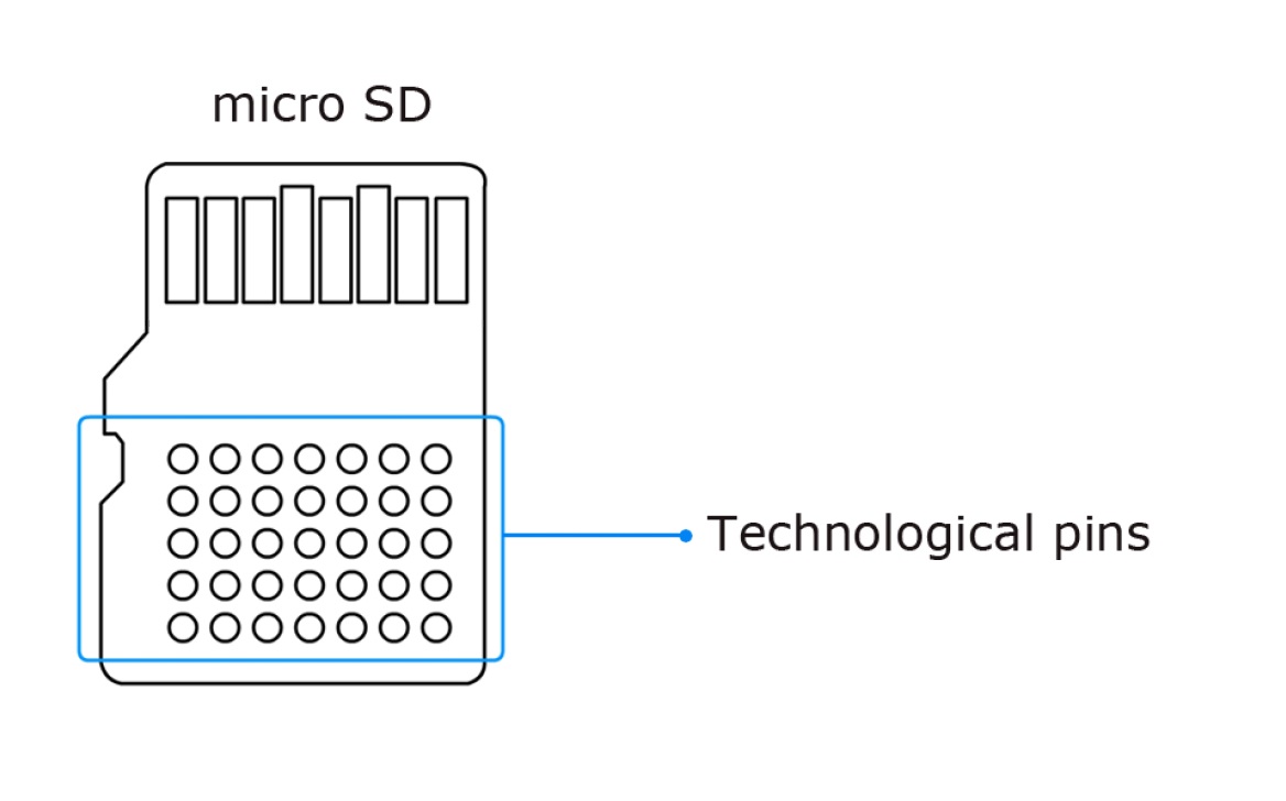
Basically, in this case we should try to find a special technological pinout on the bottom side of our monolithic device by erasing the ceramic layer of coating.
Before you start dealing with monolithic recovery, we should warn you that the complete process of monolithic device soldering is complicated and requires good soldering skills and special equipment. If you never tried to solder monolithic devices before, it’s better to try your skill on some donor devices where data is not important. For example, you can buy a couple of them just to test your skills of preparing and soldering.
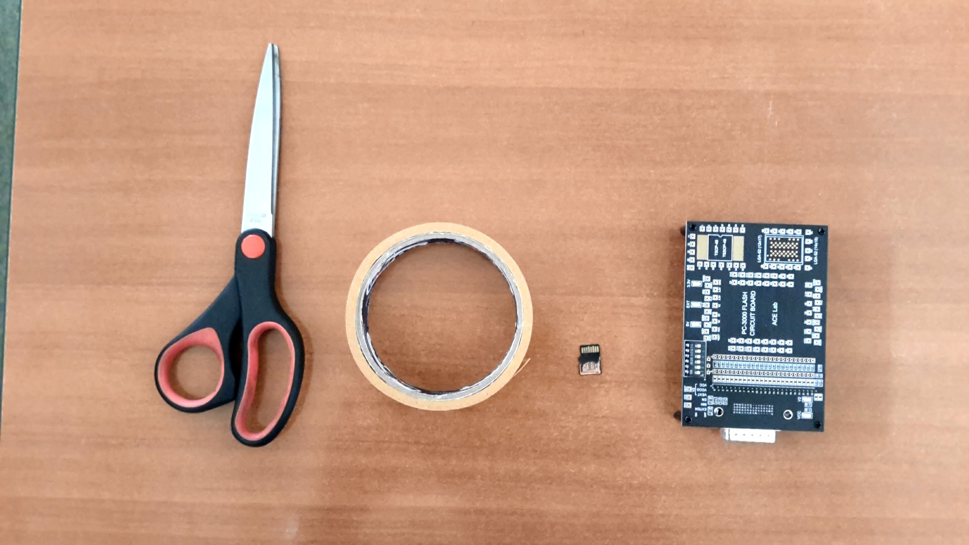
Below you can find the list of necessary equipment:
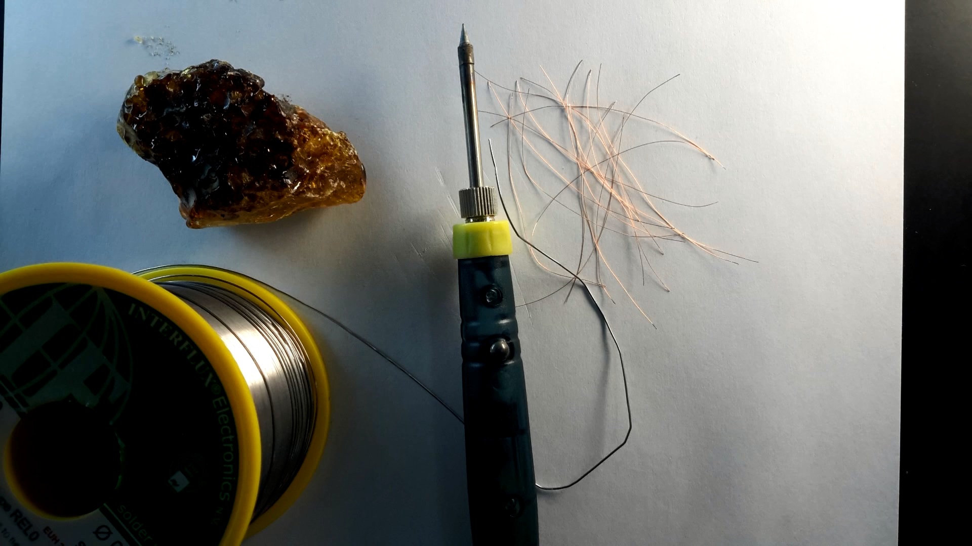
- A good optic microscope with x2, x4, x8 zoom;
- USB soldering iron with a very thin solder tip;
- Double-sided adhesive tape;
- Liquid active flux;
- Thick jelly BGA flux;
- Hot air gun station (for example – Lukey 702);
- Rosin;
- Wooden tooth picks;
- Alcohol (75% isopropil spirit);
- Copper wires with 0.1 mm diameter with a layer of isolation lacquer;
- Jewellery sandpaper (with the size of 1000, 2000 and 2500 (the bigger is the value – the smaller is the sand));
- BGA balls with the size of 0.3 mm;
- Tweezers;
- Sharp scalpel;
- Pinout scheme;
- PC-3000 Flash Circuit Board adapter or Multiboard adapter;
When all the equipment is ready for soldering, we can start our process.
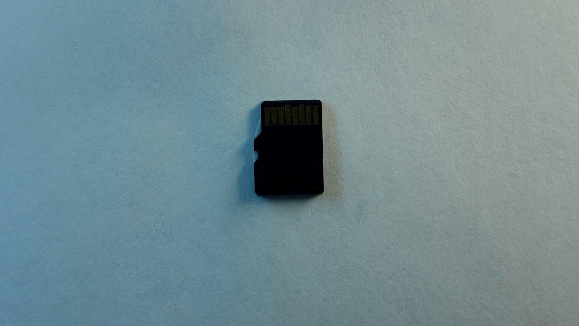
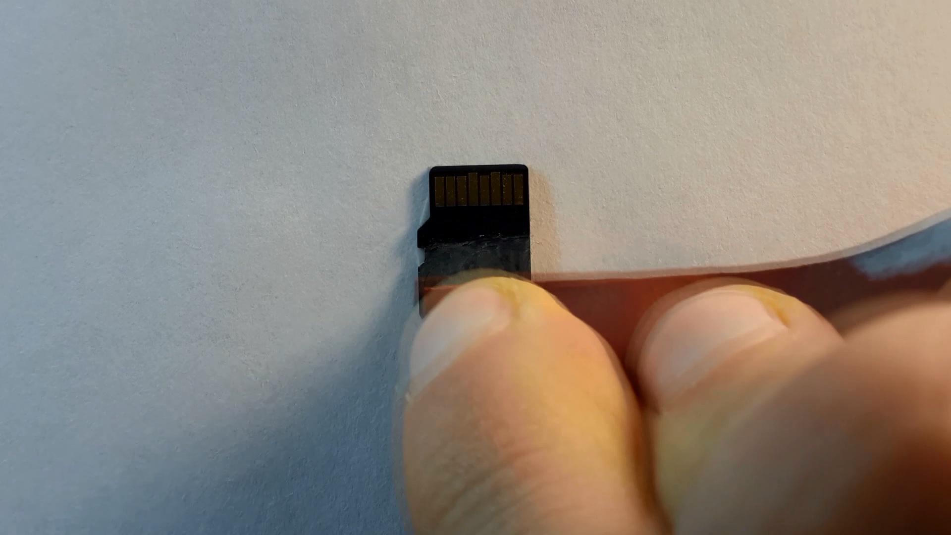
First of all, we take our monolithic device. In our case, it is small microSD card. We need to fix this card on the table with a double-sided adhesive tape.
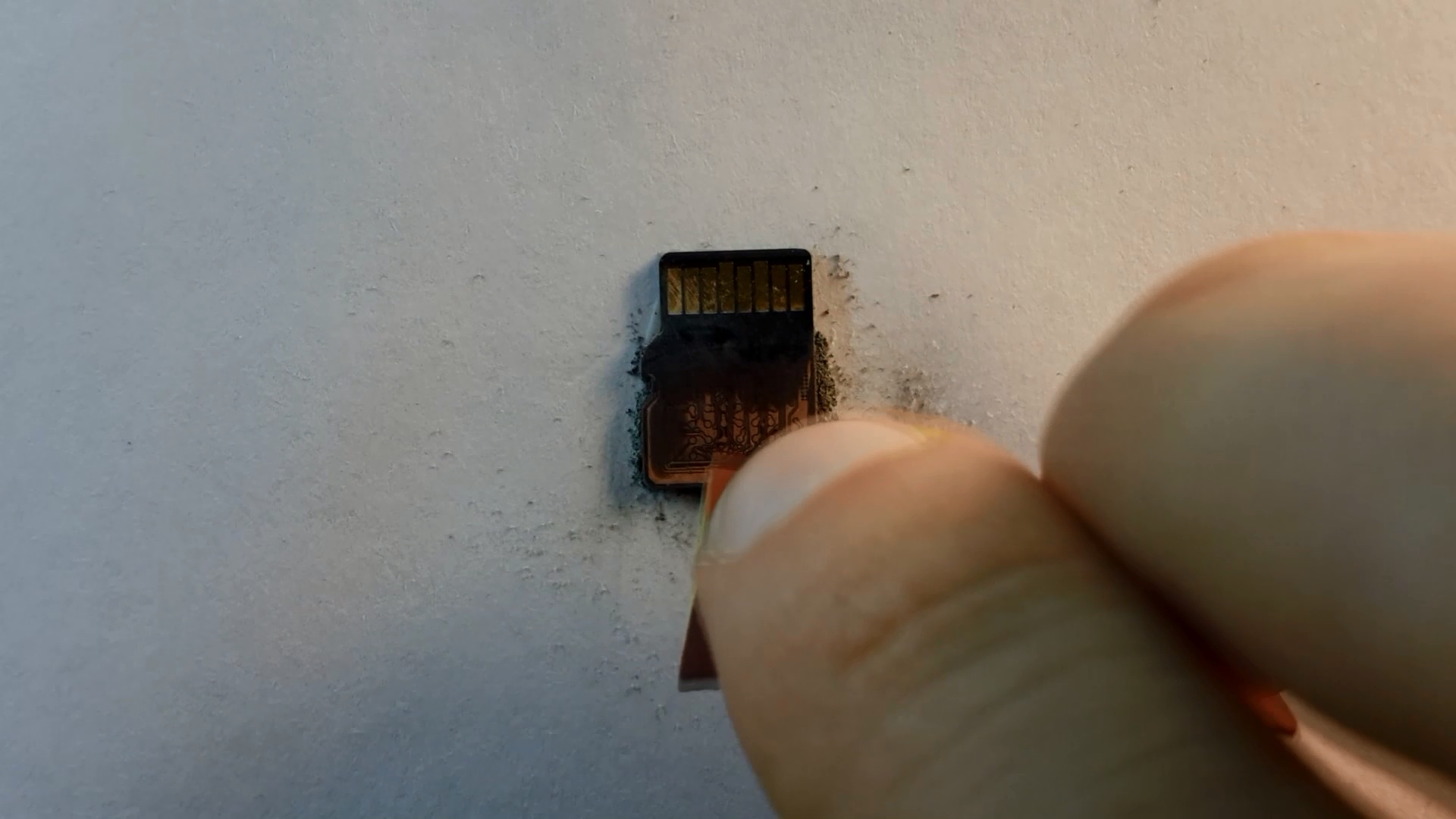
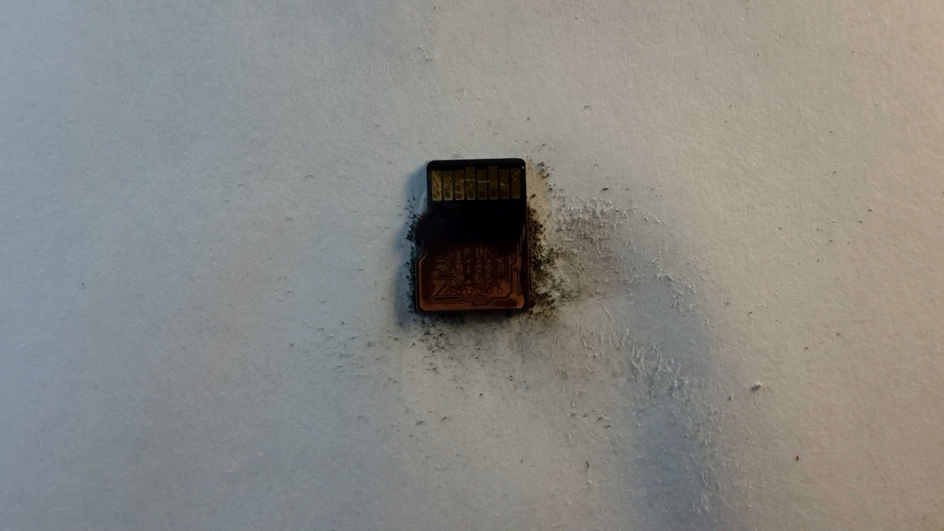
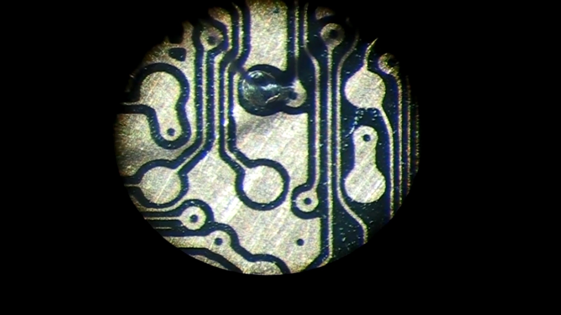
After that, we start to erase the layer of ceramic from the bottom side. This operation requires some time, so you should be very patient and careful. If you damage the pinout layer, data recovery will be impossible!
We start with the coarse sandpaper (the largest size of sand) – 1000 or 1200.
When the first largest part of coating is removed, it is necessary to change the sandpaper to the smaller sand size – 2000.
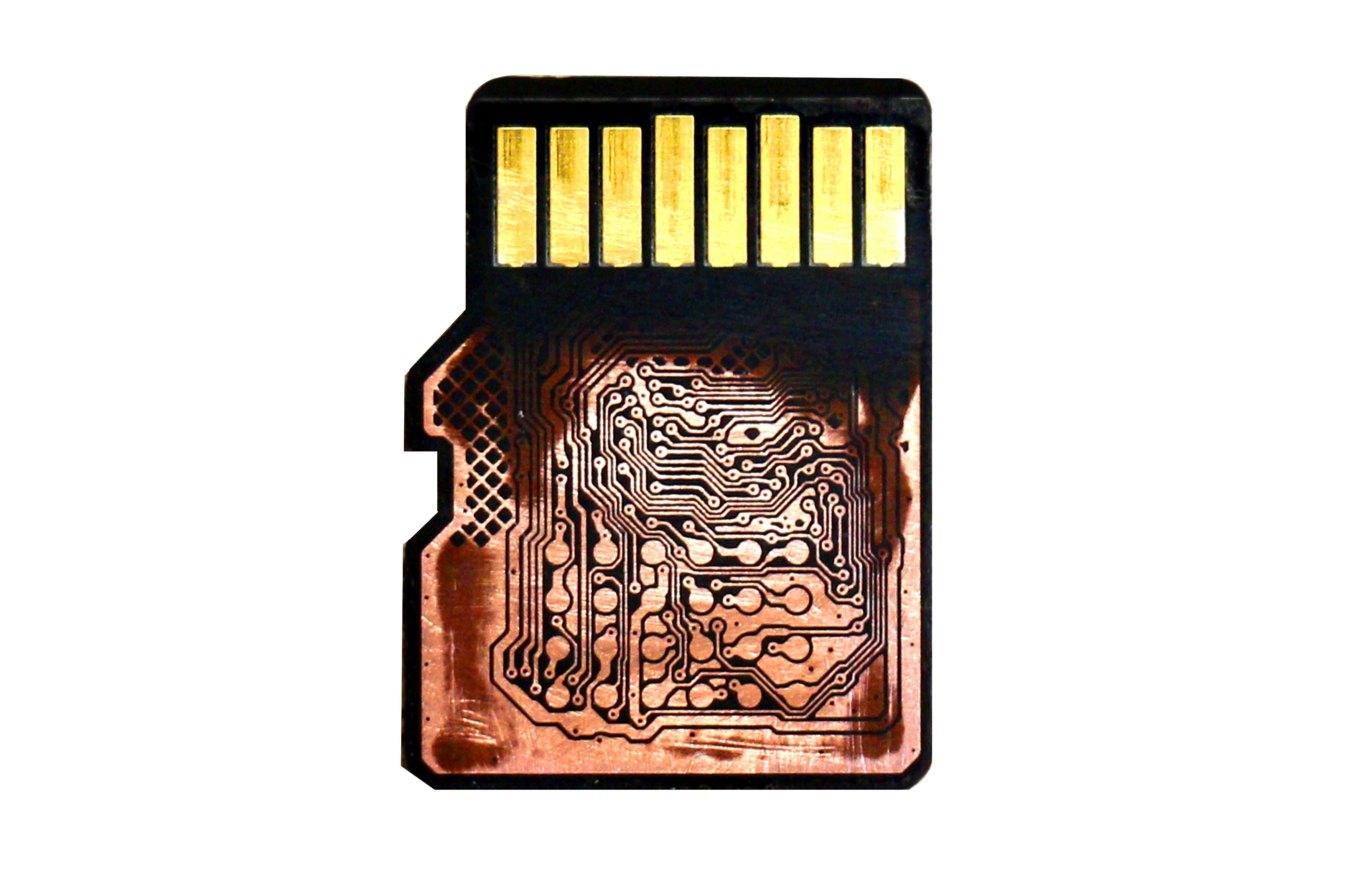
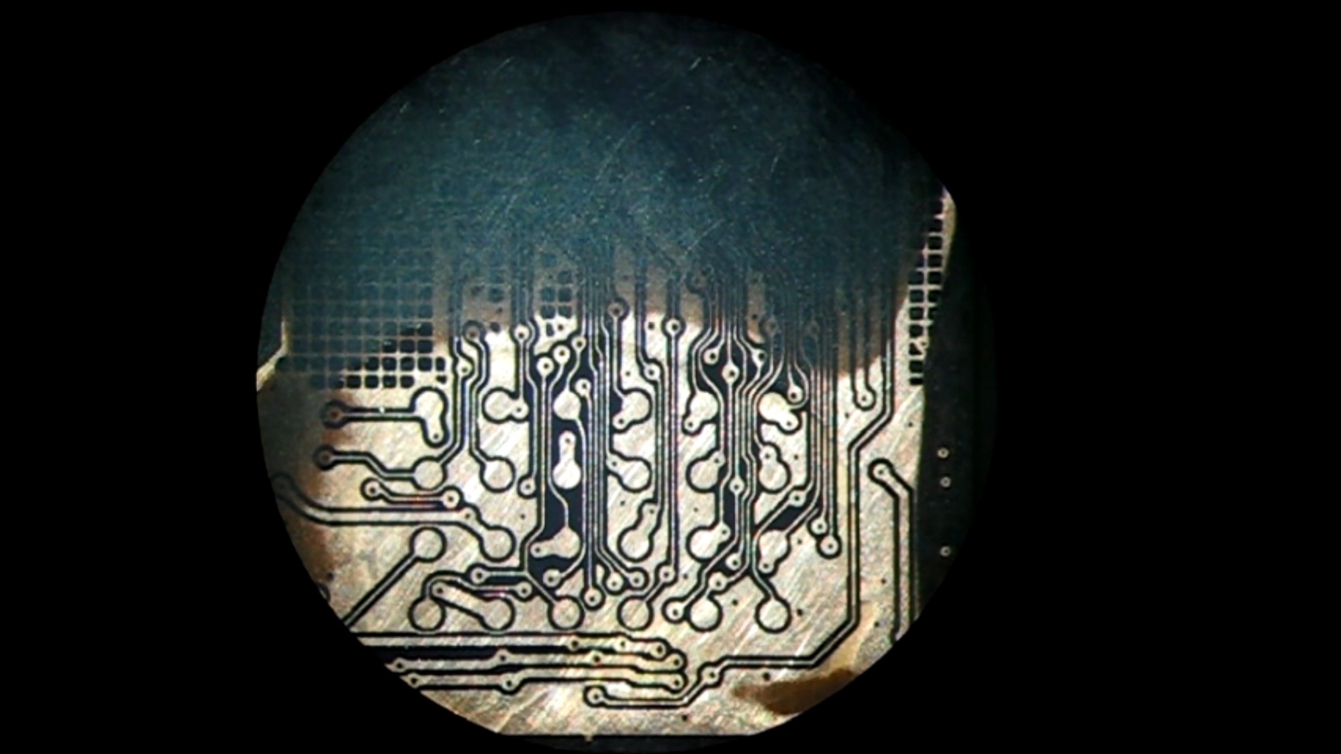
Finally, when the copper layer of contacts becomes visible, we should use the smallest sand size – 2500.
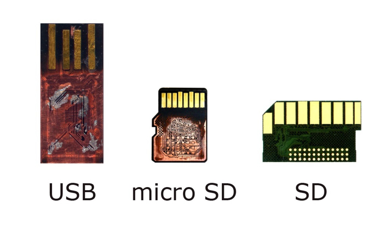
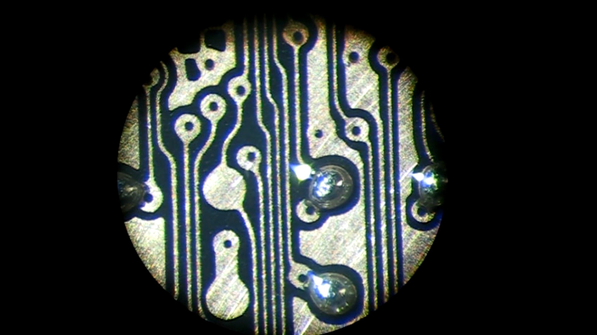
If you perform all the manipulations correctly, finally you will get something like this:
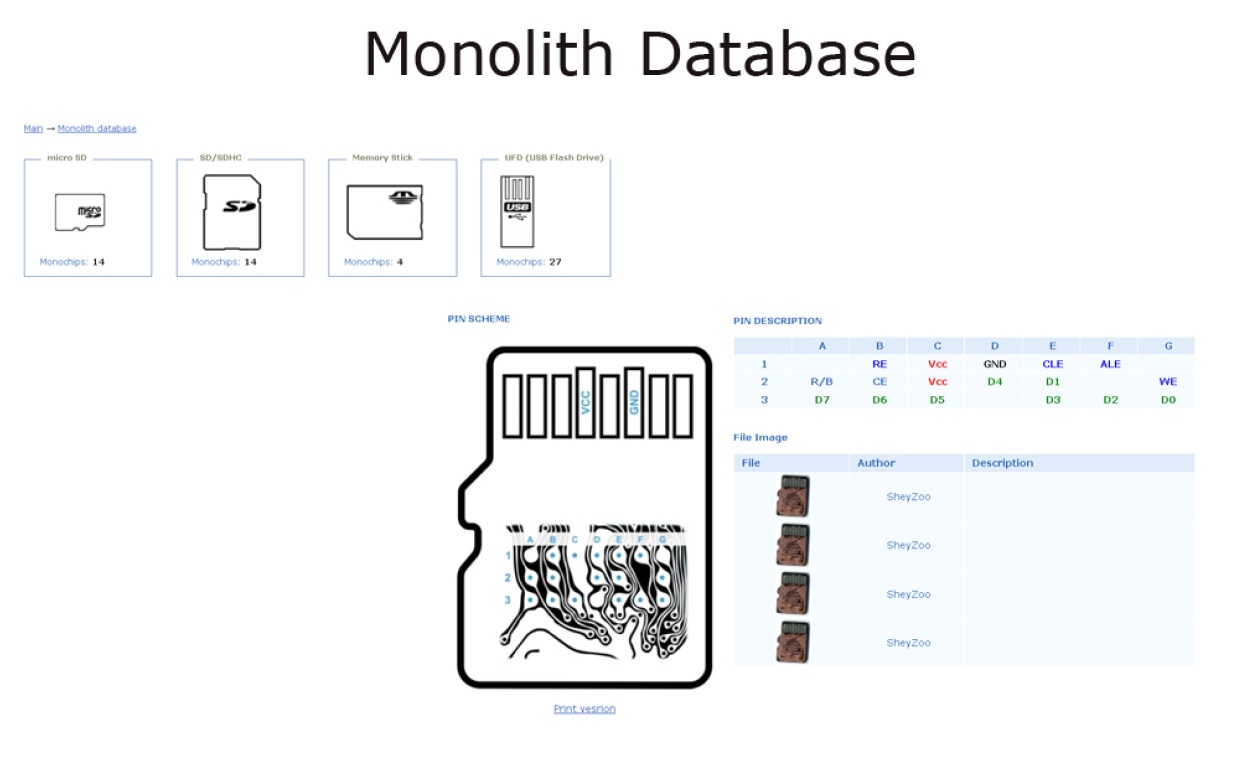
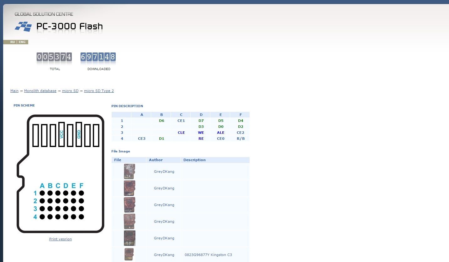
The next step is searching the pinout in our Global Solution Centre.
To continue working with the monolith, we will need to solder 3 groups of contacts:
- Data I/O contacts: D0, D1, D2, D3, D4, D5, D6, D7;
- Command contacts: ALE, RE, R/B, CE, CLE, WE;
- Power supply contacts: VCC, GND.
First, you need to choose the category of your monolithic device (microSD card in our case), and after that you have to choose a compatible pinout (type 2 in our case).
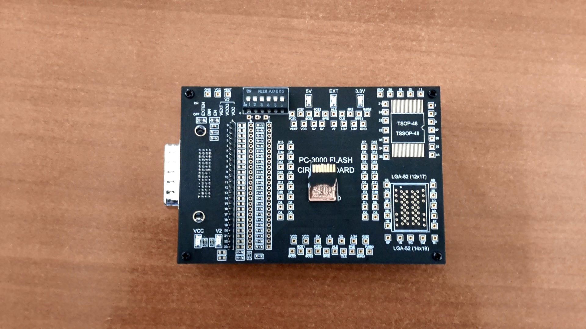
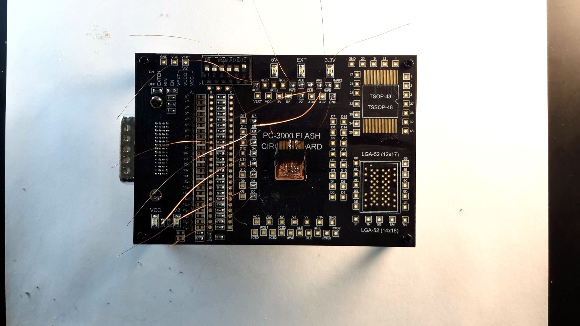
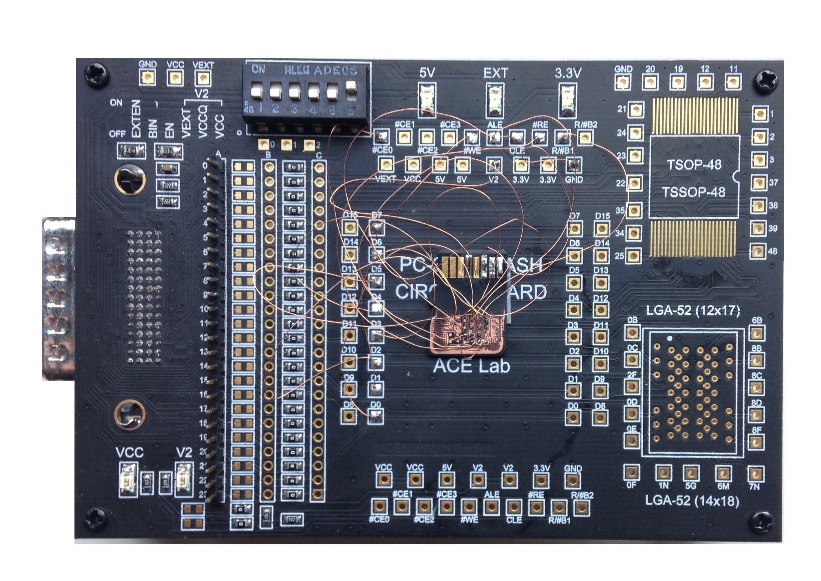
After that, we should fix the microSD card on the Circuit Board adapter for more convenient soldering.
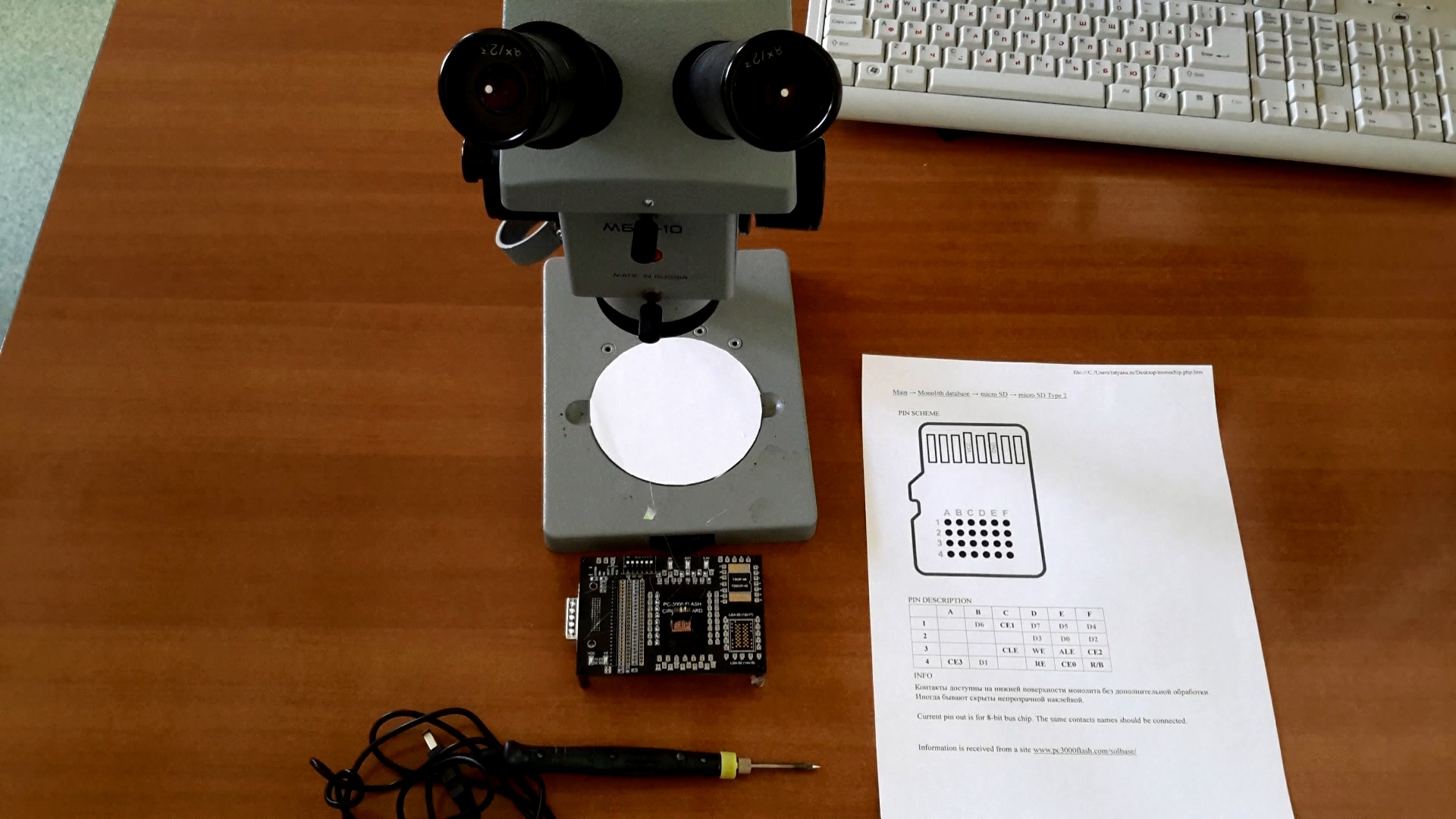
It would be a good idea to print out the pinout scheme of your monolithic device before soldering. You can put the scheme next to you, so that it is at hand when you need to check the pinout array.
We are ready to start the soldering process! 🙂 Make sure there is enough light at your workstation!
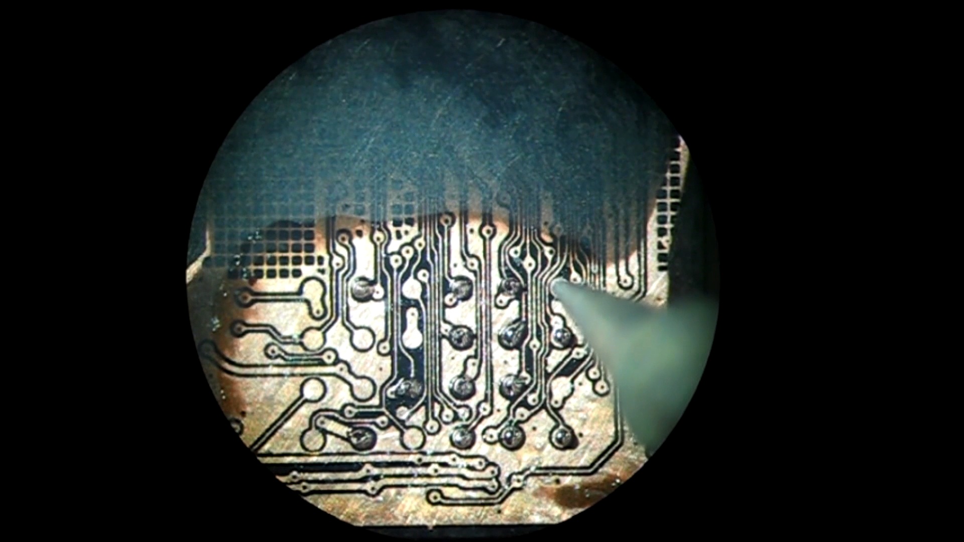
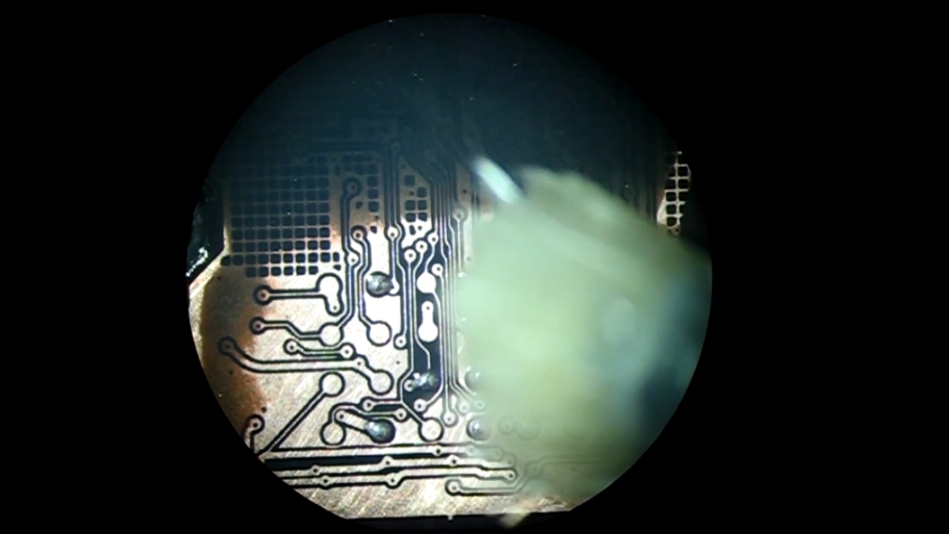
Drop some liquid active flux on the microSD pin contacts with the help of a small brush.
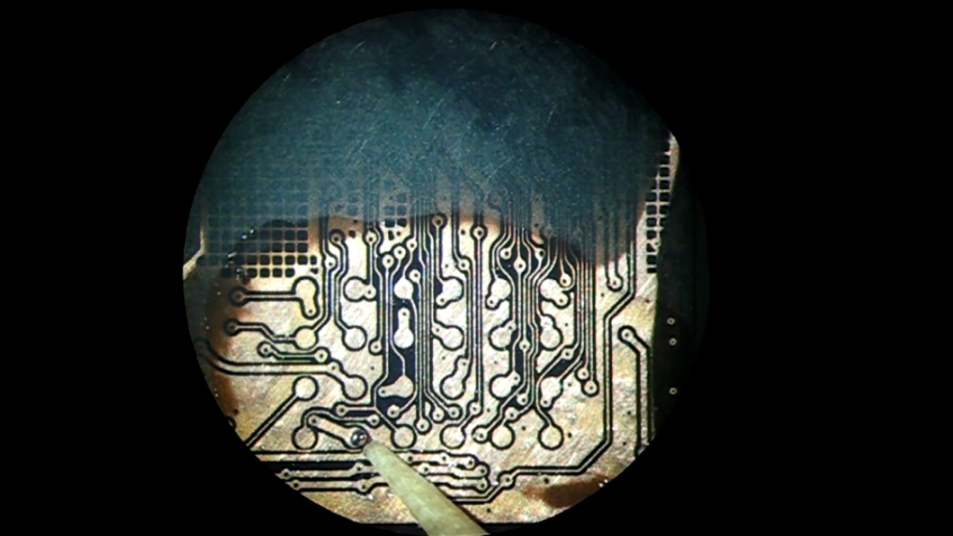
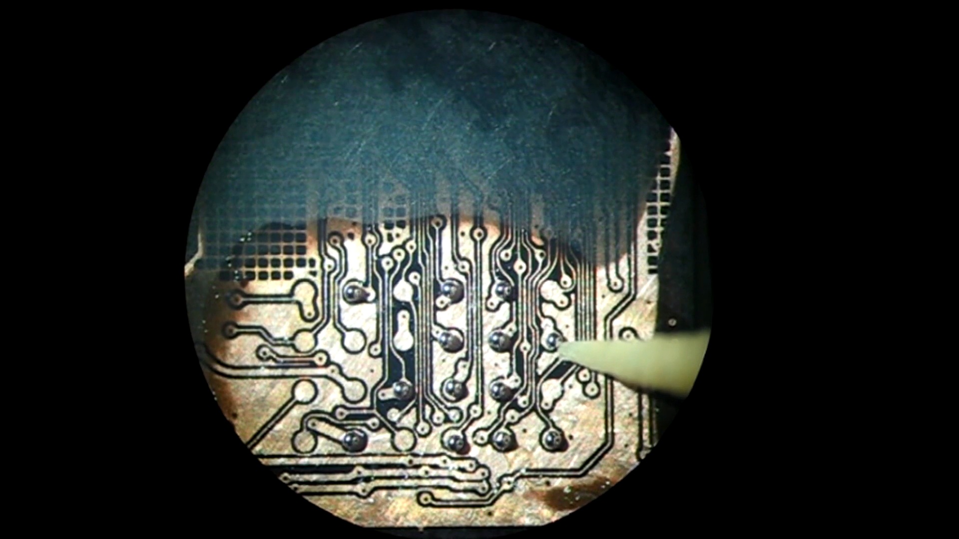
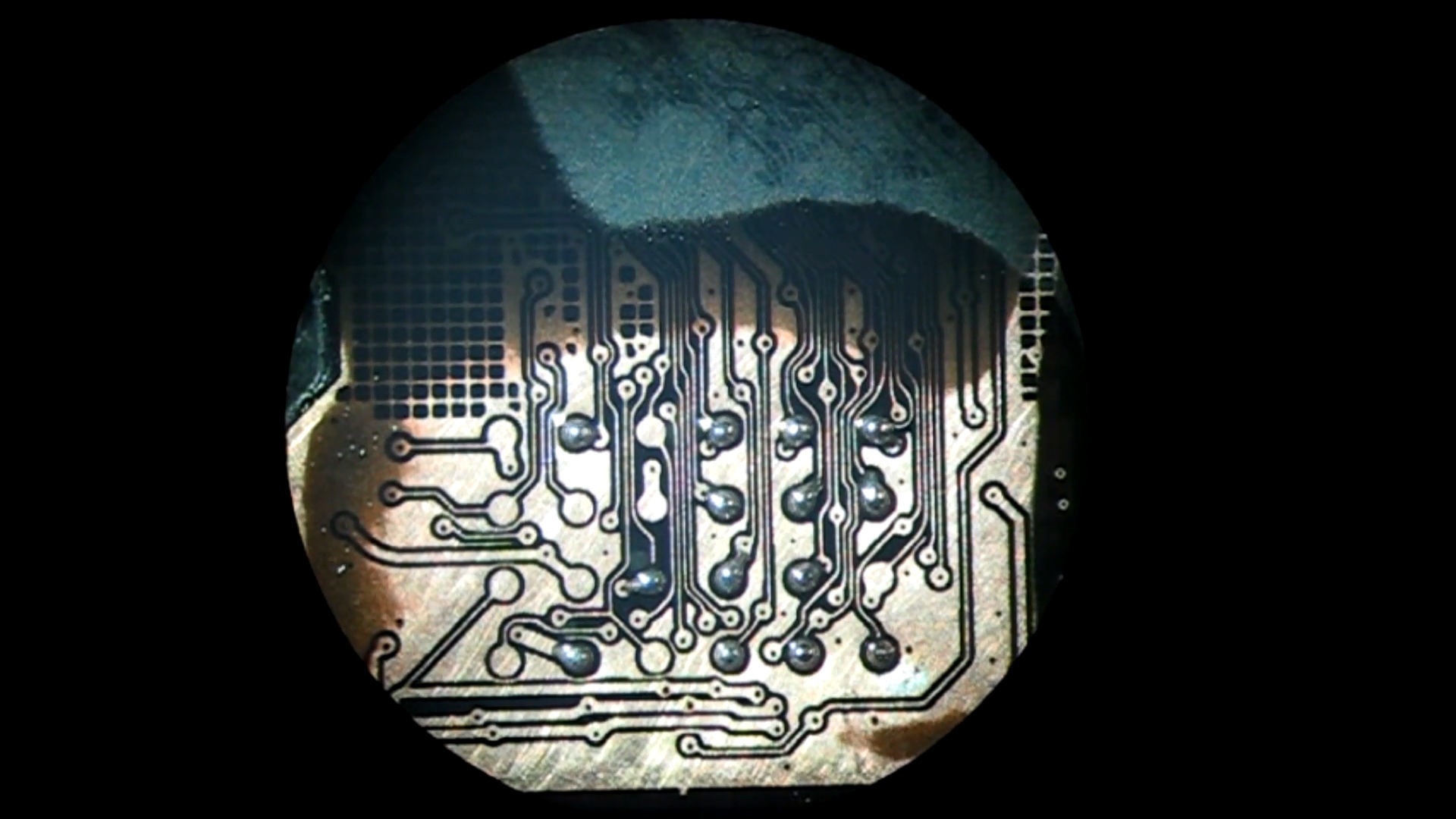
With the help of a wet tooth pick we should place all the BGA balls on the copper pin contacts which are marked on the pinout scheme. It’s better to use the BGA balls with the size of ~75% of our contacts diameter. The liquid flux will help us to fix the BGA balls on the microSD card surface.
When all the BGA balls are placed on the pins, we should use a soldering iron for melting tin. Be careful! Perform all the actions gently! For melting, touch the BGA balls with the tip of the soldering iron very quickly.
When all the BGA balls are melted, you need to put some thick jelly BGA flux on the contacts.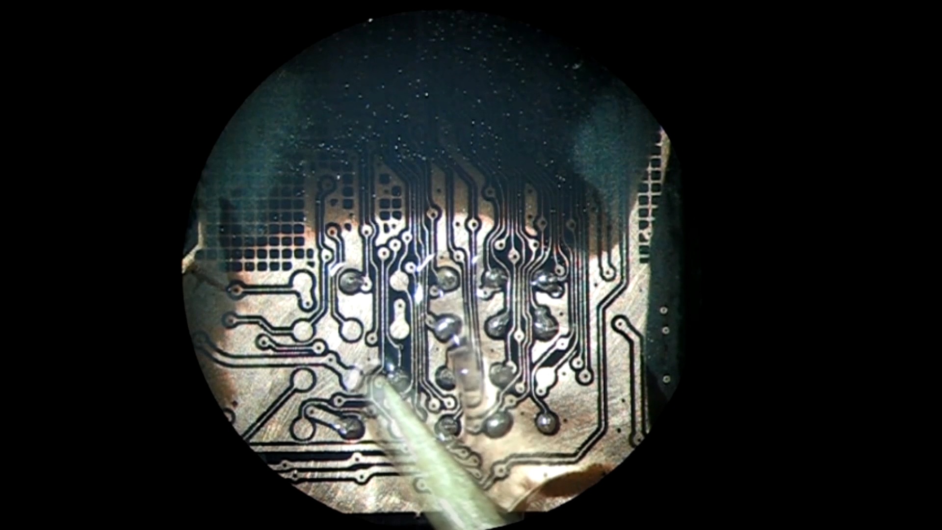
Using a hot air gun, we should heat our pins with the temperature of +200C. The BGA flux will help to distribute the heat between all the BGA contacts and melt them carefully. After heating, all the contacts and the BGA tin will take a semi-sphere form.
Now we should remove all traces of flux with the help of alcohol. You need to sprinkle it over the microSD card, and clean it with a scrubbing brush.
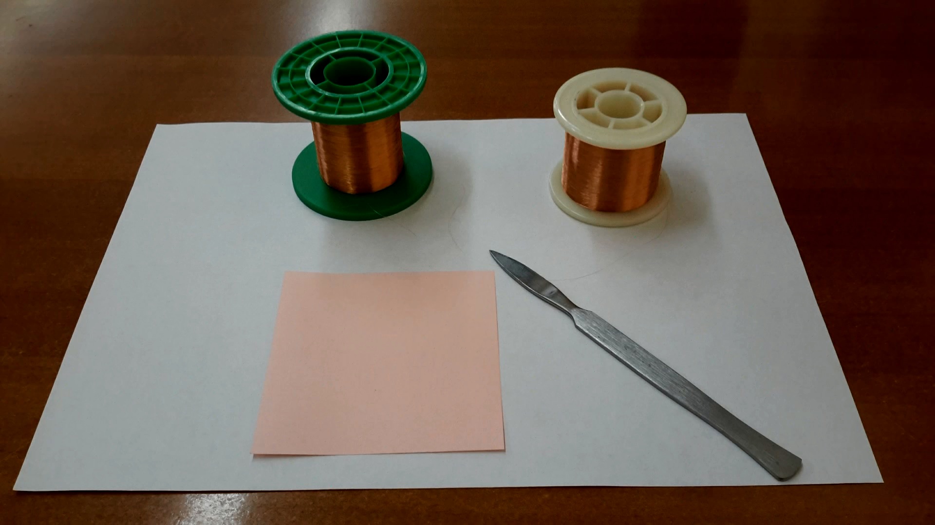
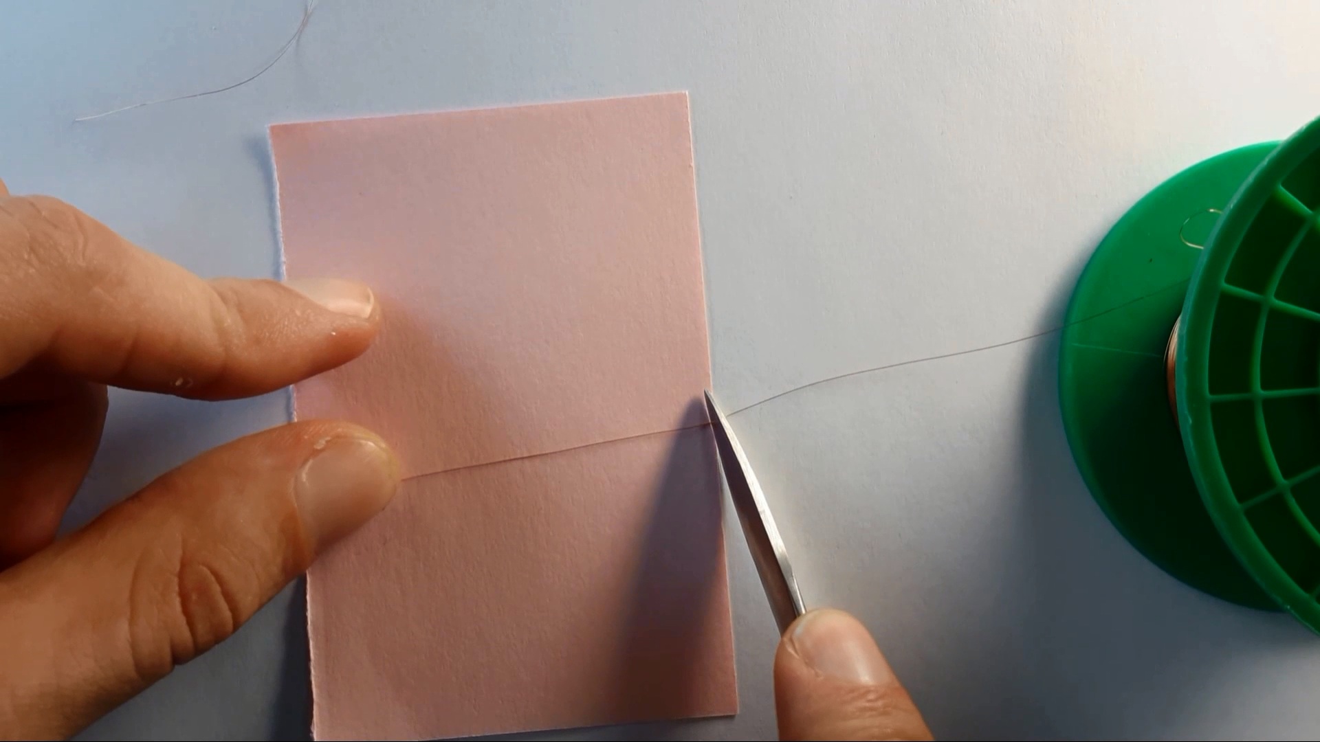
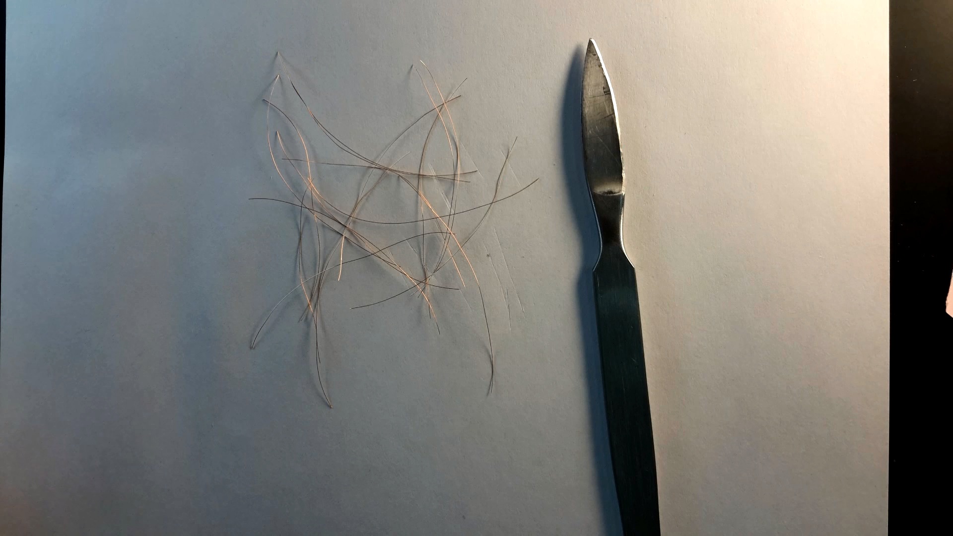
The next step is to prepare the cooper wires. They should to be of the same length (approximately – 5-7 cm). For cutting the same size wires, we recommend to use a piece of paper as a length gauge.
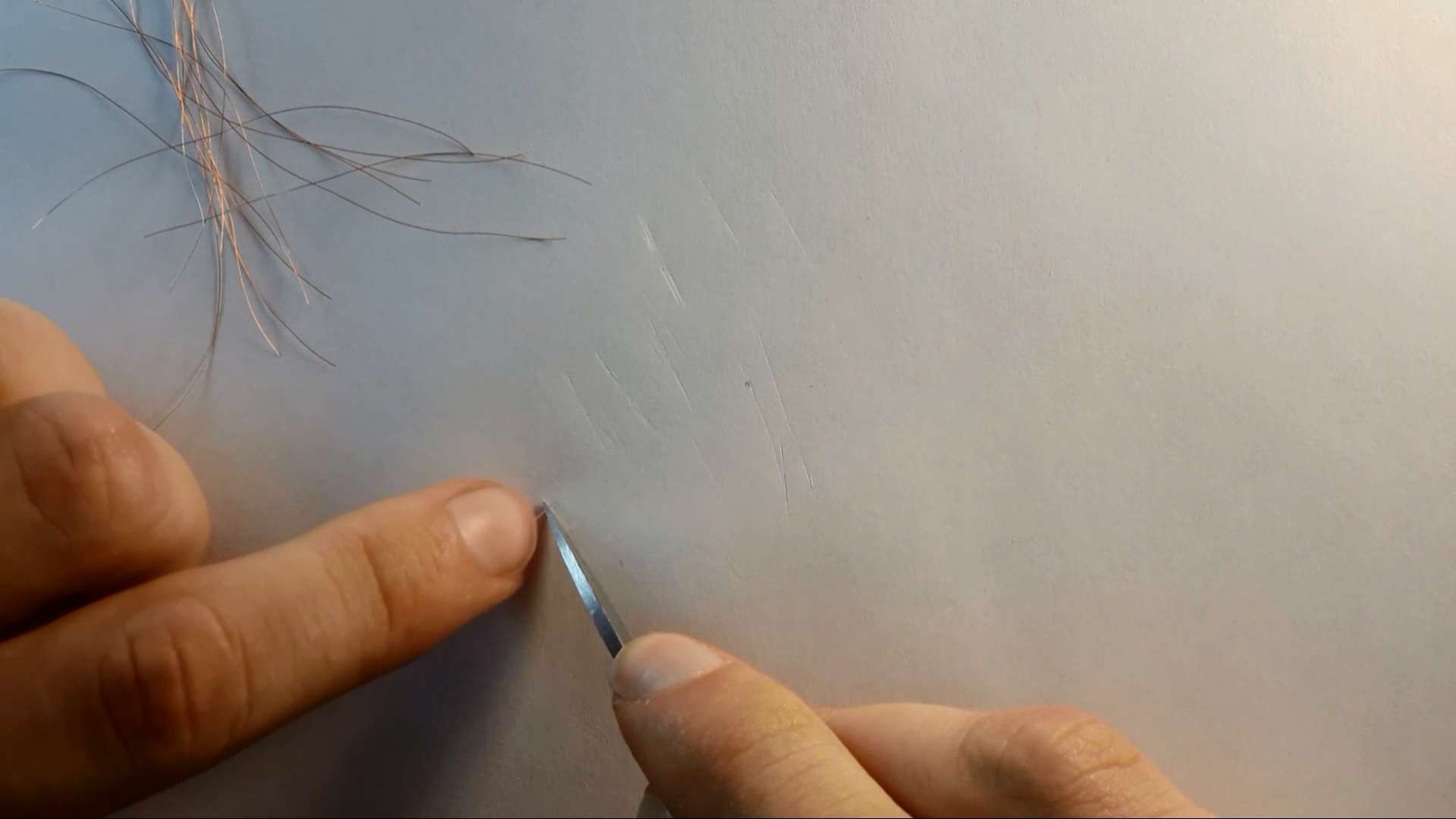
After that, we should remove the isolation lacquer from the wires with the help of a scalpel. Just scratch them slightly from both sides.
The last stage of wire preparation will be the process of wire tinning in rosin for better soldering.
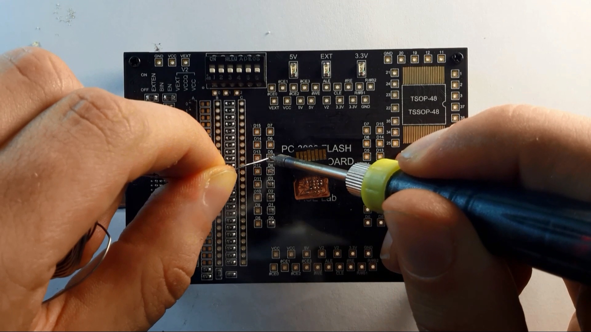
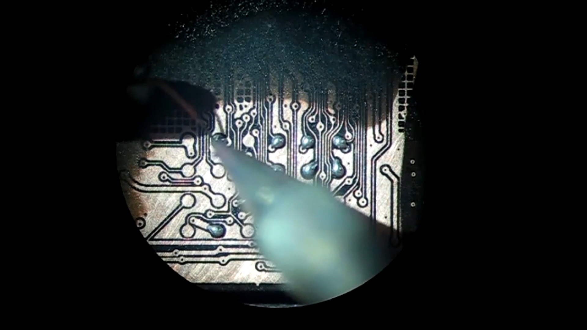
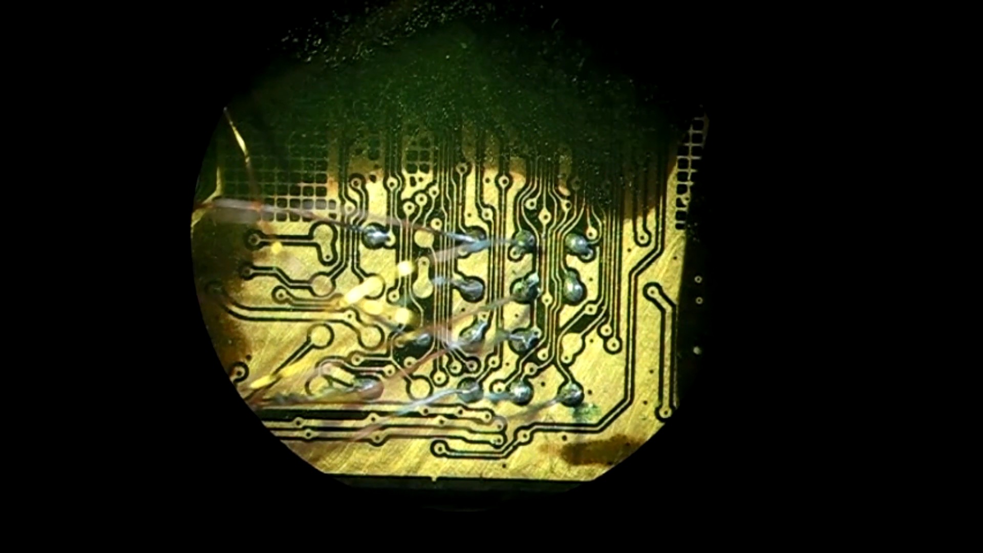
Now we are ready to start soldering wires to our Circuit Board. We recommend that you start soldering from the side of the Circuit Board and later continue soldering the other side of the wires to the monolithic device with the help of a microscope.
Finally, all the wires are soldered to the Circuit Board, and we are ready to start using a microscope for soldering the wires to the microSD card. This is the most complicated operation and it requires a lot of patience. If you feel that you are tired – take some rest, eat something sweet and drink a cup of coffee (sugar in your blood will help your hands not to shake). After that, get down to soldering. 🙂
For right-handers, we recommend that a soldering iron should be in the right hand, whereas in the left hand we hold tweezers with copper wire.
Your soldering iron should be clean! Don’t forget to clean it from time to time while soldering.
When all the contacts are soldered, make sure that no one of them is connected to the GND layer! All the pins must be fixed very tightly!
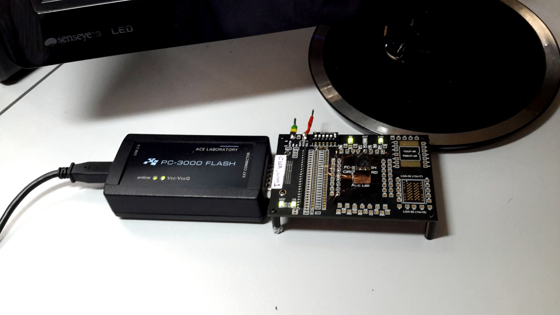
Now we are ready to plug our Circuit Board to PC-3000 Flash, and start the reading process! 🙂
Below please watch the full video:
!!!UPDATE!!!
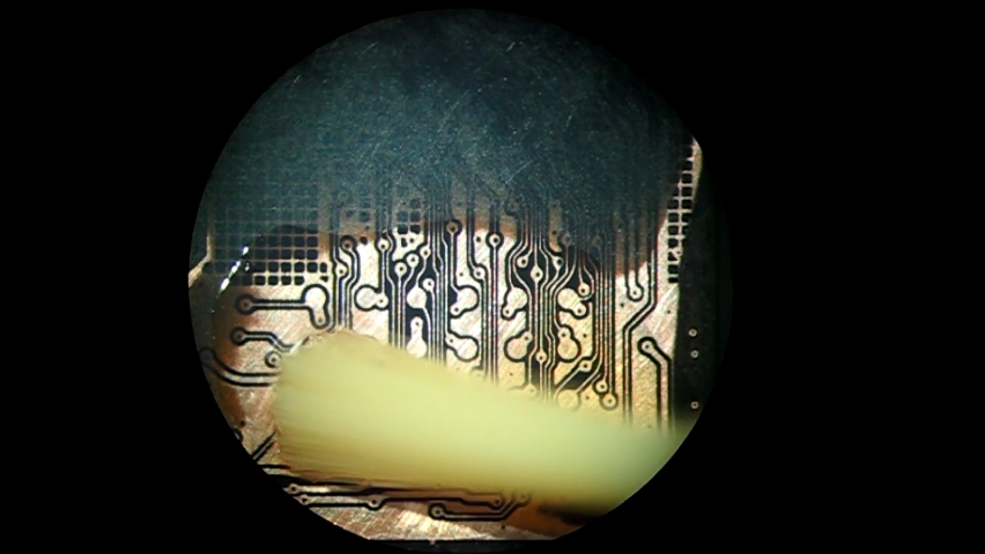
Instead SandPaper you can also use The following tool. It’s a Fiberglass brush which is perfectly clean all compaund and plastic layers, but leave cupper roads in safe!




 (8 votes, average: 4.25 out of 5)
Thank you ACE Laboratory for providing well written concise instructions on how to properly solder the pins. It is innovated approaches and shared instructions which help us better utilize your products.
Great job!
Once again ACE Laboratory clearly shows why they are far and above the best in the industry and always leading the way! Well done!
I have been performing monolith recoveries for over three years and I wish I would have had ACE when I started. The important thing is my lab now is filled with ACE Laboratory products. Although I utilize my own techniques, it’s always good to see how someone else does it. Thank you very much for the step by step process in great detail. Thank you ACE Laboratory for sharing your knowledge and engineering of the best and the brightest minds in the industry!
Text is fine, but this technique looks amateur’s. Cheap chinese tools and non professional approach. I’d invest couple hundreds of bucks for better gear if I was about to show this to pro community.
Well, if you are ready to spend 30 000$ for buying expensive equipment for monolithic device recovery – that’s really great! 🙂 From our side, we just show how to work with the most complicated cases, using absolutely cheap and truly available hardware and tools. You can bought it everywhere, and final result will be also very good – even if you don’t spend a thousands of bucks.
Totally true Admin!
A Bad Workman Always Blames His Tools.
Thanks you sir, I am from China, We have got pc3000 flash ssd, but we need to improve .so I will work hard to come blog.
Any help where I can find this stuff in the U.S? or online would be even better.
Thanks a lot
Hello! In any hardware store, it should not be a problem – there is nothing unique in it.
By the way – we recommend to use fiberglass pen instead sandpaper 🙂
Awesome article Roman! all i needed to know, Thanks.
i’ll try to remember not to solder to the sound of push the tempo 🙂
Does this method of recovery work on a microsd card (Sandisk Ultra microsd 128 GB) that is split in half, in such a way that the bottom layer where the technological pins are located is intact?
Hello! It would be nice if you will provide some pictures with bottom side of your monolith. We should understand what type do you mean.
Sure, I can provide photos of the monolith I have. I wasn’t able to upload the photos in the comments, is there another way to send them to you?
You can contact Technical support: http://ts.acelaboratory.com/
I would like to buy this tool please where I can get it I am very interested
Hello! You can contact with our sales department:
http://www.acelaboratory.com/order.php
Hello,
i have Sandisk Extreme 64GB Card.
The Card is only recognized as a 32mb card on Windows Explorer.
Unfortunately the card is getting pretty hot!
Do you think i should try Recovery or is this impossible?
What Eqipment do i need?
The soldering part is no problem. But i need the hardware and software tools!
Thank you very much!
Hello,
Most likely – it’s a firmware corruption. Probably Translator Tables become bad, and that’s why you can see only 32MB capacity. If your SD card is a monolith, you can try to recover it with the help of PC-3000 Flash and Spider Board. For more details – please send email to Max, he will guide you: sales@acelab.eu.com
great article. thanks for sharing .
is there any softwear for firmwire flashing etc..
i searched alot but cant find firmwire files of sdcard .. as i know sdcard contain rom and processer so is there anyway to dump softwear inside rom
Hi. My sdxc card was recently broken into two. I do not know if the memory chip is still intact. I seriously need help to recover very important data in it. Please get back to me asap thank you.
If your SDHC is a monolith then recovery will be impossible. If it contains a common BGA or TSOP chips inside and they are in a good condition – it will be possible to recover it.
Hello, Im confused, did you not retrieve data from an sdhc card monolith type in the example above….
This example shows how to read dump from mSD card. Other steps of recovery are pretty simple. The most complex part – is soldering to Circuit Board.
Repairing monolith where *only* the contact half is broken can be achieved, sometimes (as others mention) it can be connected to. Slight problem is that without a reference point determining pinout can be very difficult.
Also many newer cards use controller to determine physical location within the Flash so data can “seem” garbled unless cloned bitwise to an identical card.
I have one here with possible NASA data on it, still haven’t had much luck but seems to have a good Flash chip according to meter tests.
By following this post one can know the updates and functioning of the SD card and the development it has gone through with its first manufacture. Very informative article.
In a cellphone bloke by UI sistem. It is posible to access to the memory and recovery the data images? Wiring the bus data parallel in order a flash data memory?
It depends. If we are talking about mSD recovery – it would be possible if content on mSD will be not encrypted by phone OS.
It’s a great content