Compact Flash cards – are the most fastest memory cards in the market. The main secret of CF – is a very powerful controller, which has direct access to several physical memory chips, which are placed on the CF PCB. The architecture of Compact Flash controllers is much closer to SSD CPU than to common USB Flash drive controllers.
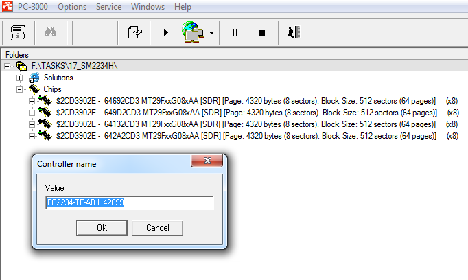
One of the most popular Compact Flash card controller is Silicon Motion SM2234H. Usually this controller works with 4 physical memory chip, and provide a high speed of reading and writing operations.
When customer get the recovery task based on this controller, he make a wrong steps of recovery and usually never get a good result. In this article we will try to explain, how to deal with this controller, and what exactly you should do for getting user data from such case!
First of all – we should remember, that SM2234H split the data between 4 physical chips, and before we will see any file headers, we should make several steps.
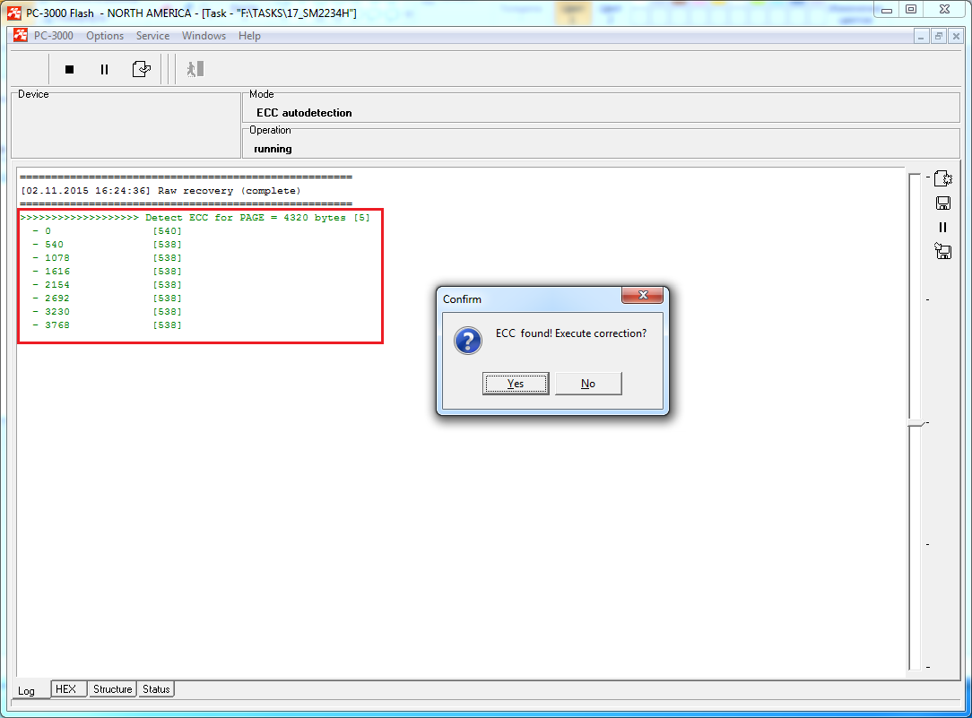
- When all memory chips will be read, launch ECC autodetection and fix all bit errors on all chips!
- After that, we should change the order of our memory parts.
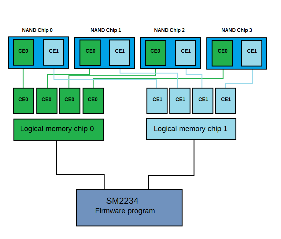
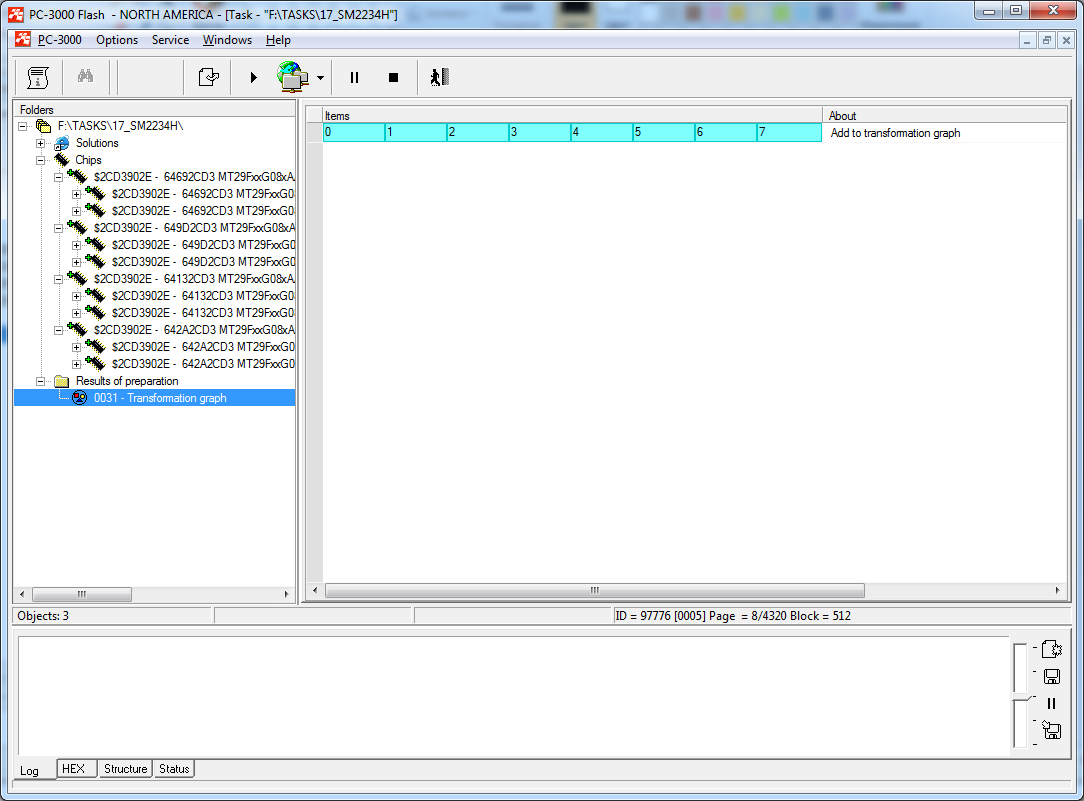
In current case we have 4 physical chips with 2 logical parts in each memory with the complete order of parts: 0, 1, 2, 3, 4, 5, 6, 7;
All even parts – will be first parts of our chips: 0, 2, 4, 6;
All odd parts – will be the second parts of our chips: 1, 3, 5, 7;
SM2234H firmware program see all this parts like a 2 logical chip arrays, and all writing operation with blocks and pages will be performed with this virtual logical memory chips. Controller, at the same time will split all data by bytes, and will placed data in each CE part.
If we need to write for example, the word: RECOVERY, controller will split the whole word by bytes: R, E, C, O, V, E, R, Y, and than – will write:
R – to Part 0 (NAND 0, CE0) Virtual logical memory 0
E – to Part 2 (NAND 1, CE0) Virtual logical memory 0
C – to Part 4 (NAND 2, CE0) Virtual logical memory 0
O – to Part 6 (NAND 3, CE0) Virtual logical memory 0
V – to Part 0 (NAND 0, CE0) Virtual logical memory 0
E – to Part 2 (NAND 1, CE0) Virtual logical memory 0
R – to Part 4 (NAND 2, CE0) Virtual logical memory 0
Y – to Part 6 (NAND 3, CE0) Virtual logical memory 0
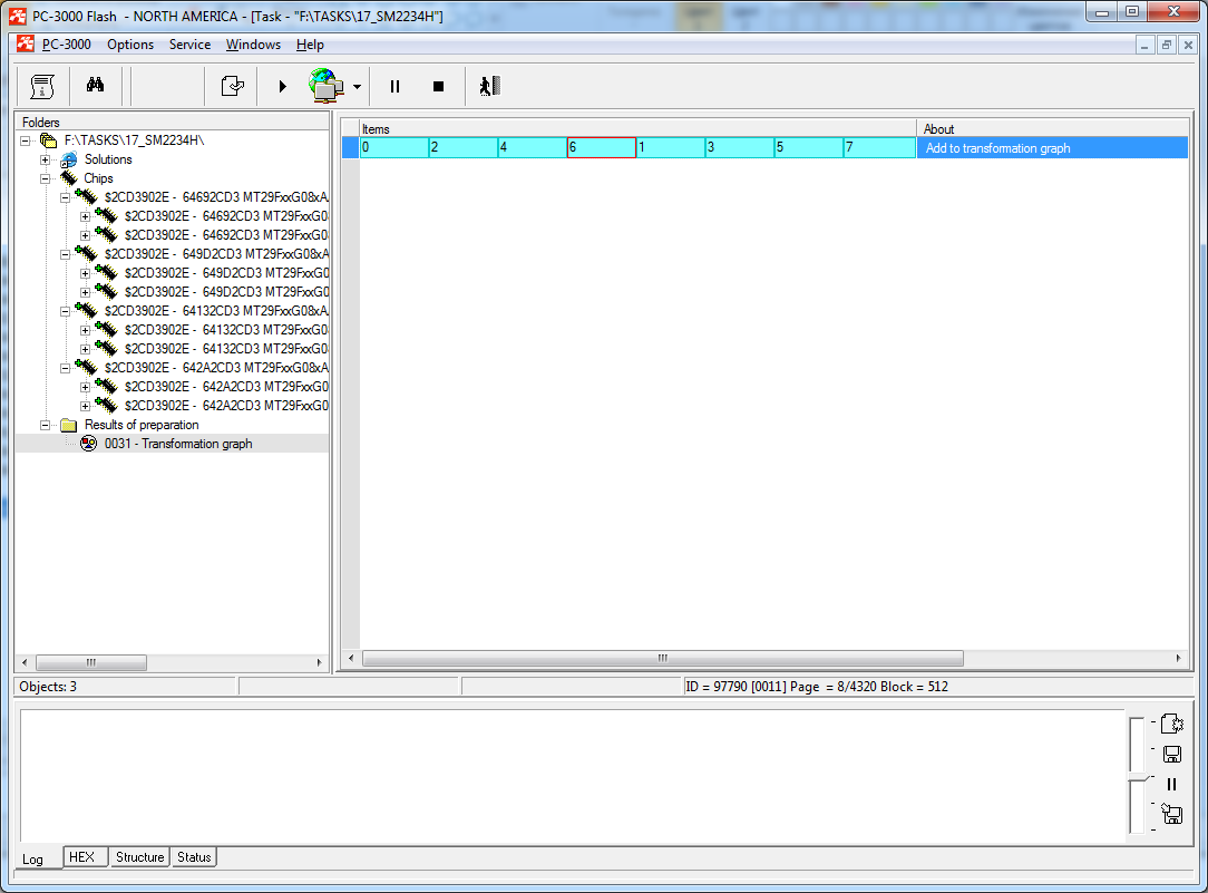
That’s why we need to change order of parts from default:
0, 1, 2, 3, 4, 5, 6, 7 to
0, 2, 4, 6, 1, 3, 5, 7
We should’t forget about real memory chip order! We remember that this order is very important, and we need to use Ux marking of chips on PCB during NAND unsoldering and reading. In our case we have only dumps, we don’t know real order. So, what should we do?
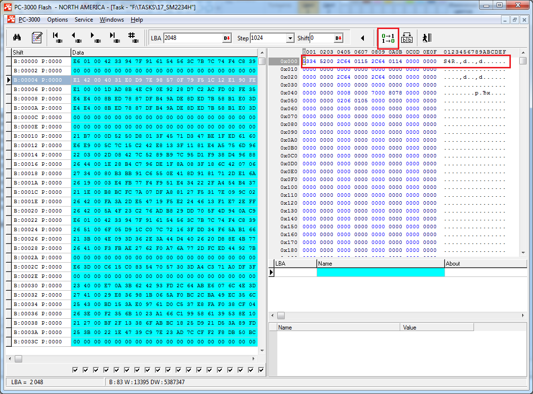
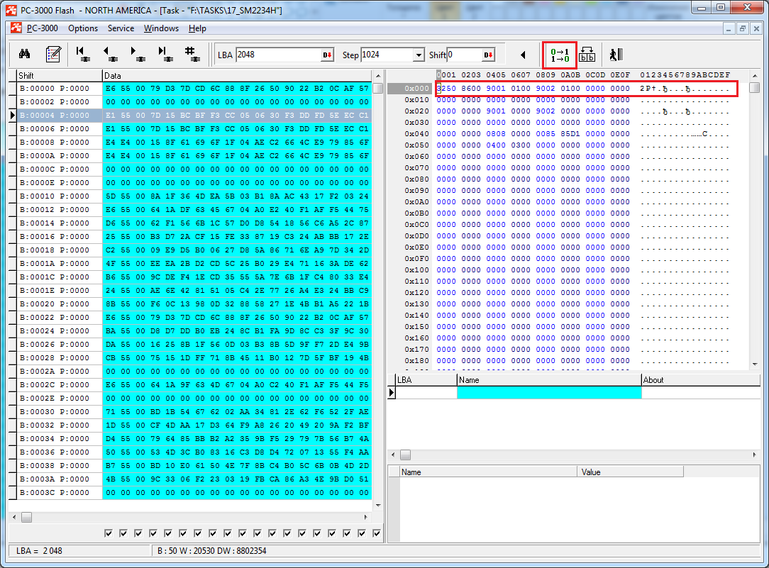
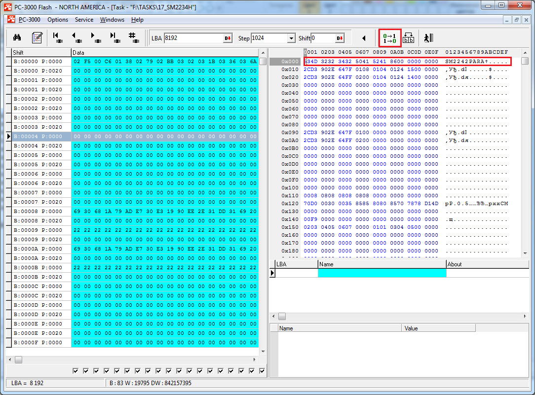
Exist one very interesting way, how to detect memory chip order in SM2234H controller. If we will check first bytes in first blocks of every parts in Service Information tool: 0, 2, 4, 6, we will see a parts of bytes: S4R, M2A, 2P, 2A.
If we will join all parts together, we will get our controller name: SM2234PARA.
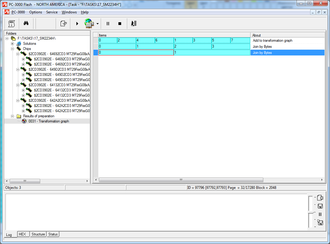
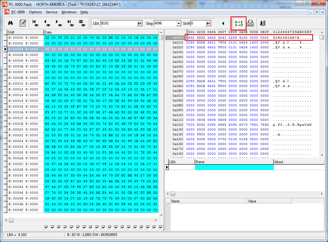
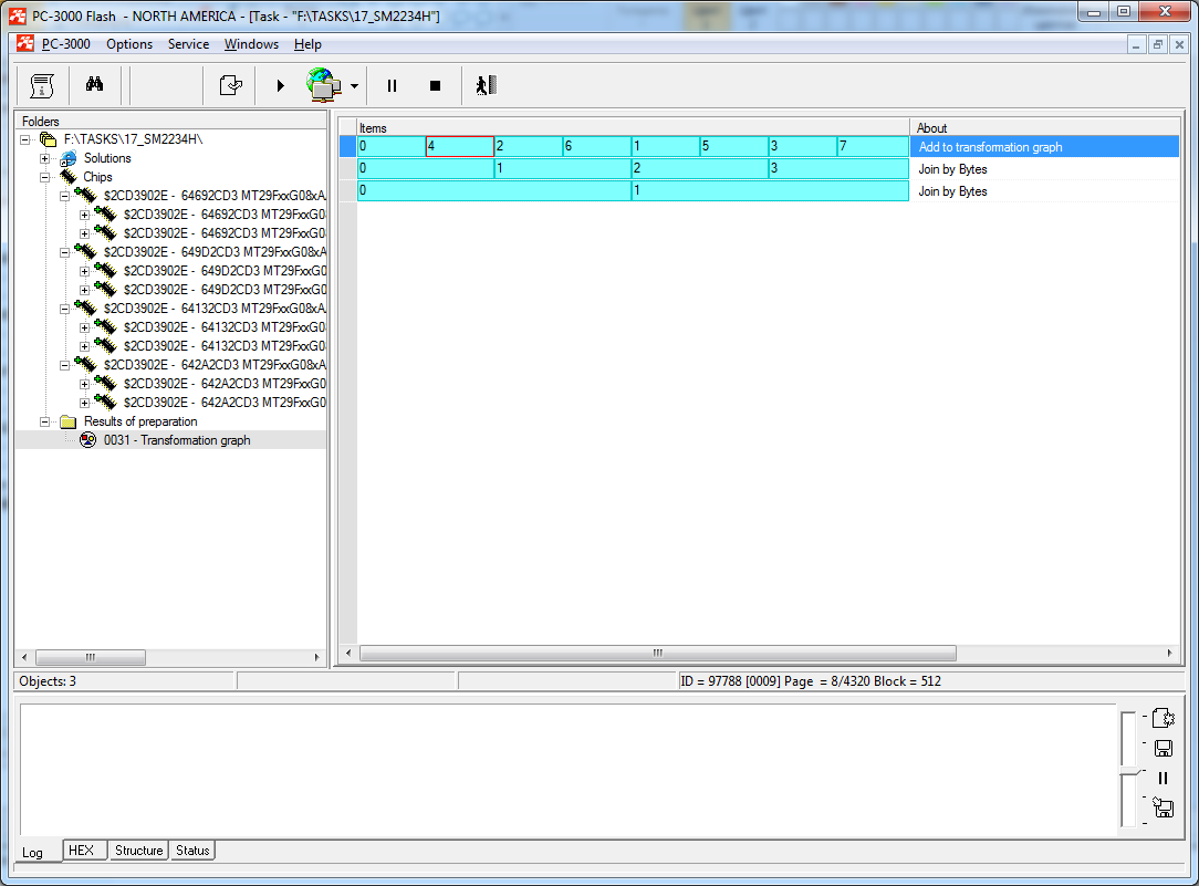
We make two join by bytes operations, and get the following result:
Unfortunately instead a correct marking SM2234PARA, we can see S2M24P2ARA. It means that something goes wrong, and parts are not set correctly.
PLEASE, REMEMBER! IN ALL SM2234H cases, correct order of markings MUST BE:
Part 0 – S4R
Part 2 – 2P
Part 4 – M2A
Part 6 – 2A
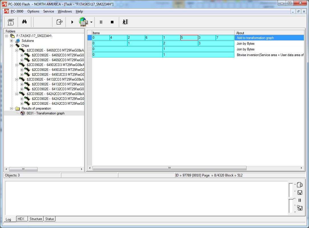
That’s why we should change the order of our parts to: 0, 4, 2, 6, 1, 5, 3, 7
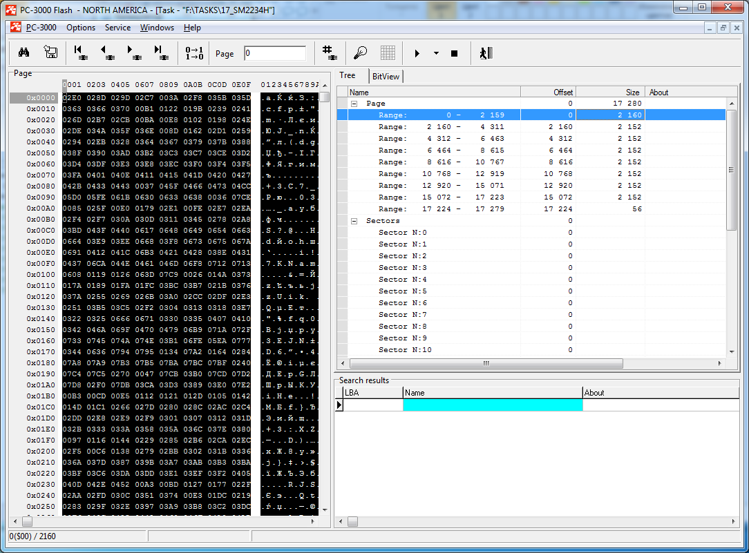
Next step – page transformation. In this case ECC autodetection will help us to apply correct page transformation!
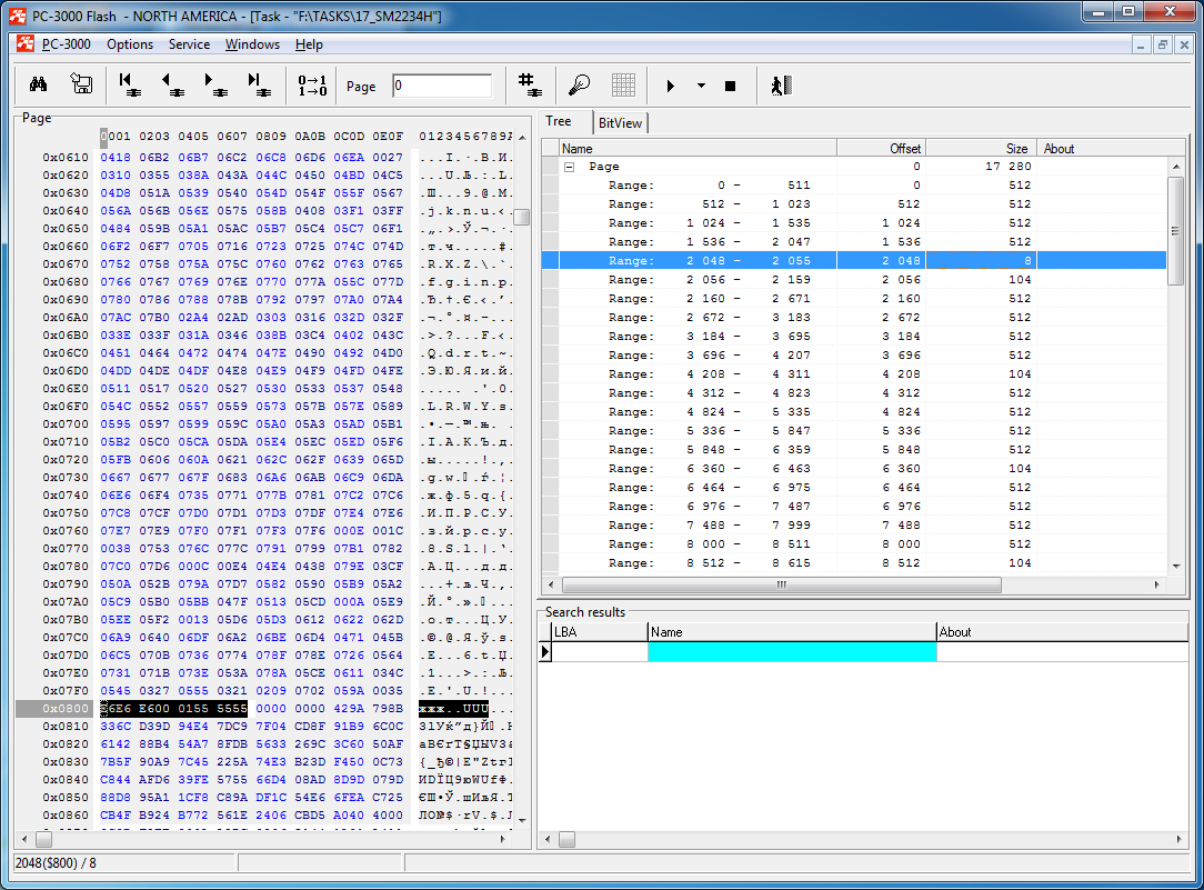
First range is 540 x 4 = 2160 (we make two joining by bytes, our ranges increase in four times)
All other ranges are 538 x 4 = 2152;
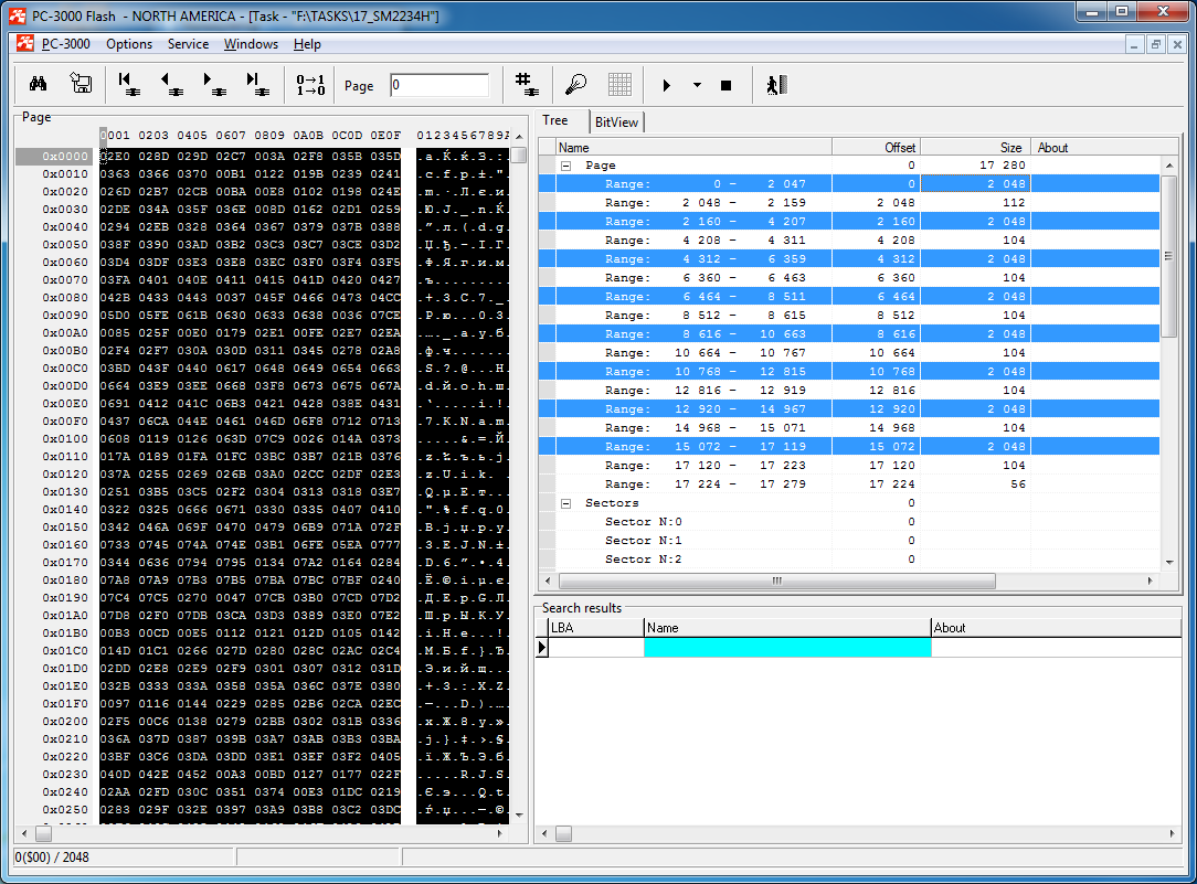
Splitting all our ranges disproportionally on 2048 (4 sectors with 512 bytes of DA):
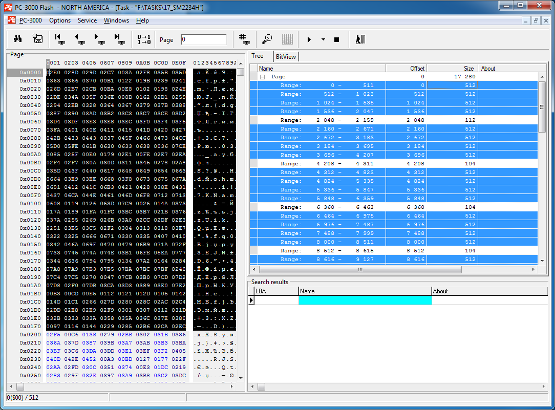
Splitting our DA with 2048 bytes for 4 parts: 512+512+512+512:
Now, we need to get the SA Marker, which contain information about block number. Add this 8 bytes to all 512 DA ranges, and apply this structure:
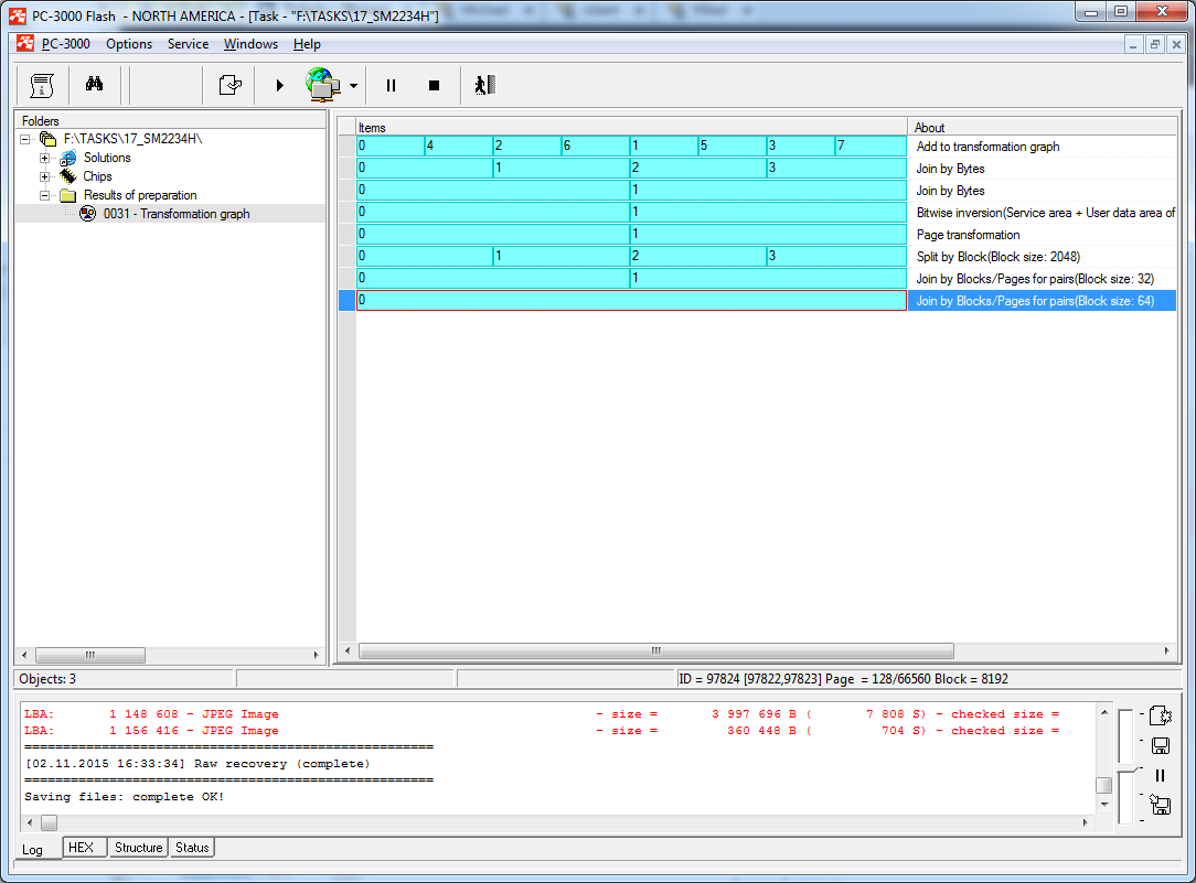
Applying interleave elimination and joining by bytes for pairs:
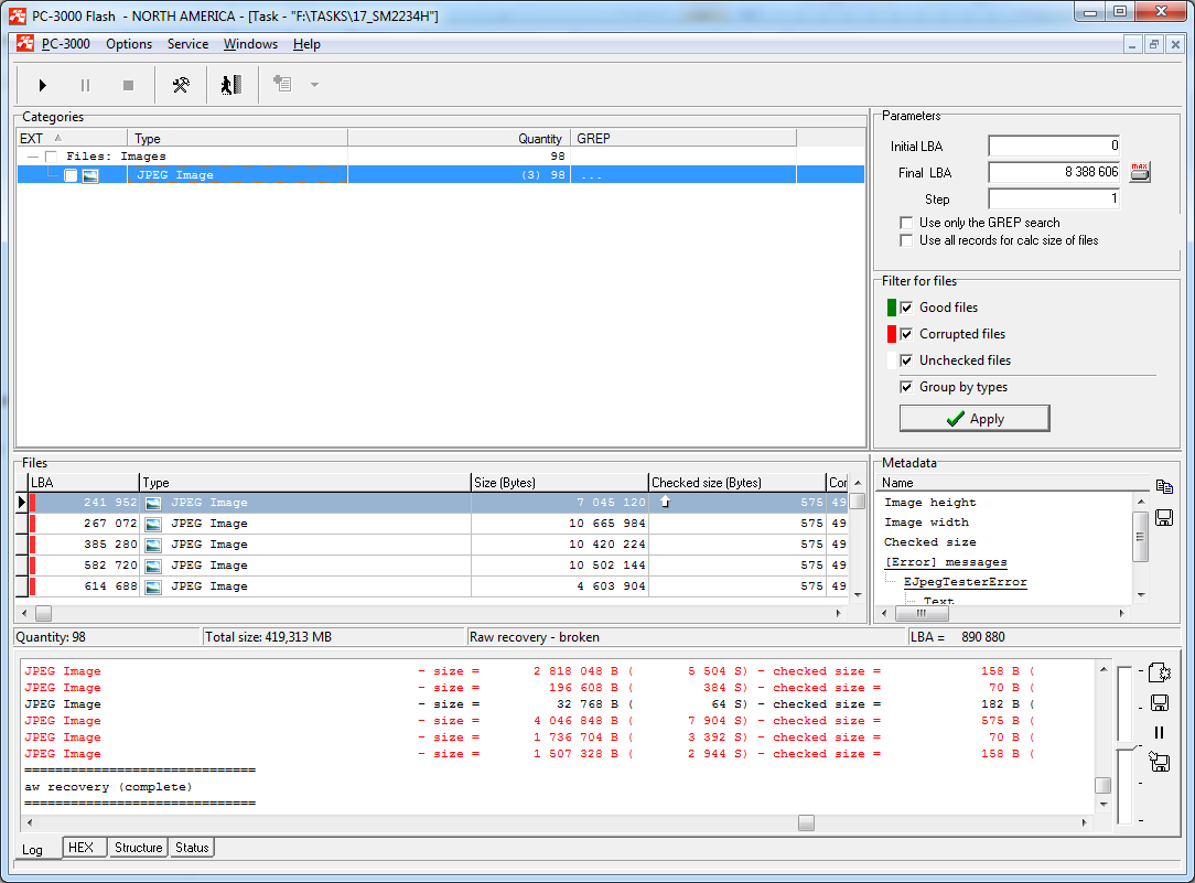
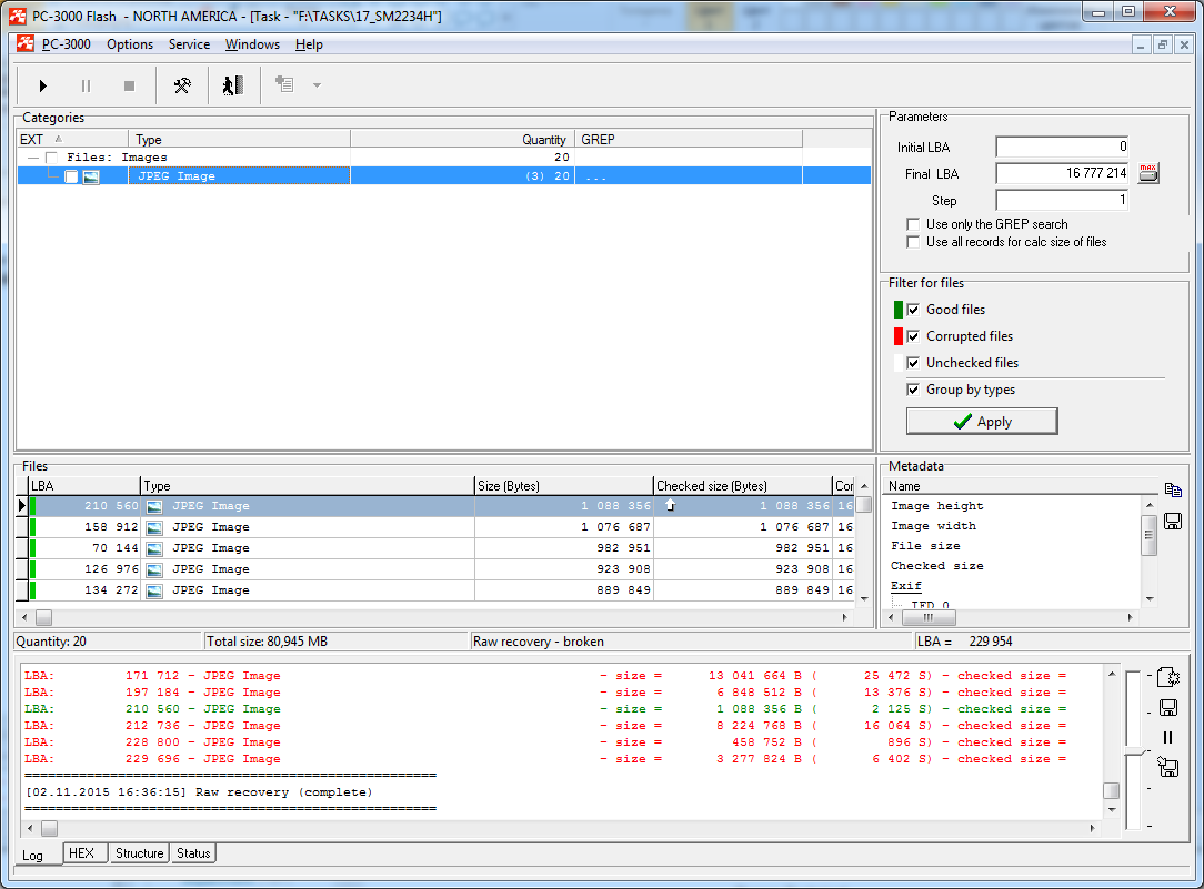
Starting RAW recovery:
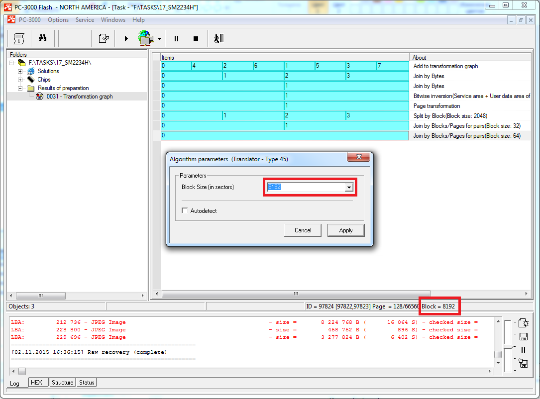
And building image with translator Type-45 SM2234H:
That’s all! 🙂
And again, a couple of important rules:
- Don’t forget about good chip order using Ux marking during chip unsoldering;
- Don’t forget to apply ECC after chips reading;
- First parts of memory chips should be on one side of transformation graph, second part – on the other side (like 0, 2, 4, 6 and 1, 3, 5, 7).
- Check the marking of SM2234H controller name in all parts! Chips should be in the following order: S4R (part 0), 2P (part 2), M2A (part 4), 2A (part 6)!
- Use ECC for page transformation!






thanks a lot of information keren