In this article we will try to describe the optimal way for NAND memory chip unsoldering in TSOP-48 or TSOP-56 package. Before you will start the whole procedure of unsoldering, you must be sure that you have all required tools, enough time and patience! 🙂
This procedure is very important for further data recovery. If you will overheat chip – cells inside memory might be destroyed, and the number of bit errors will seriously grown up. If you will not heat the contacts well enough, you can damaged them during chip removing and make your further recovery very-very complicated or even impossible.
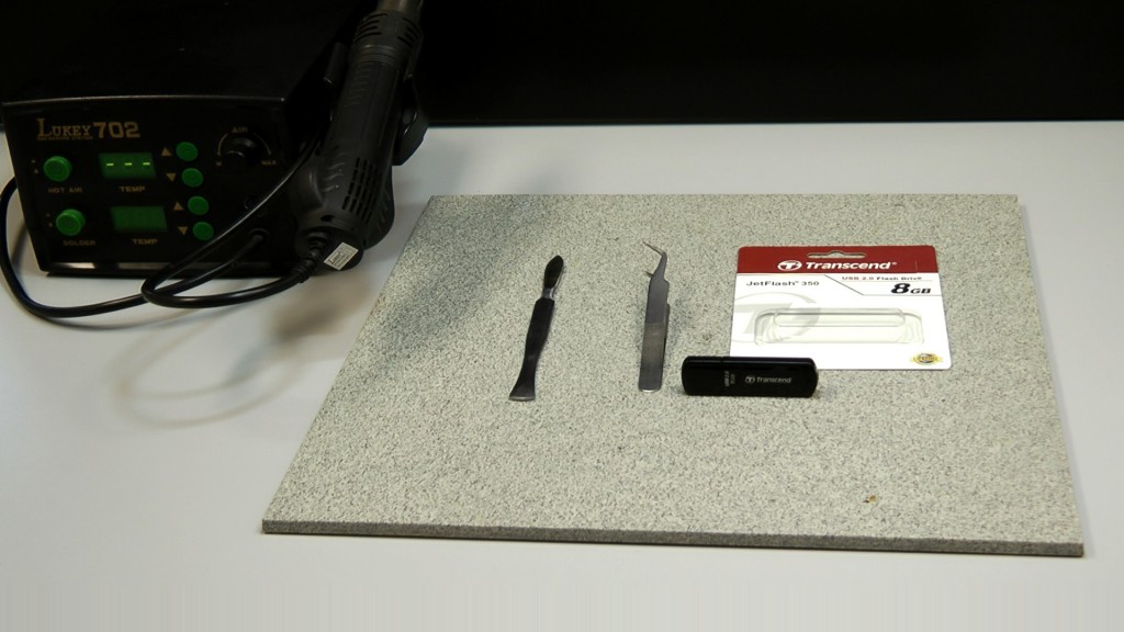
During chip unsoldering, we recommend to use the following tools:
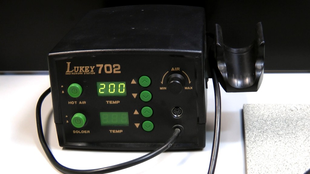
- Hot Air Gun station (we are using Lukey 702);
- Piece of ceramic plate where we make all soldering operations;
- Tweezers;
- Sharp scalpel.
During unsoldering we are not recommend to use infra-red heat stations, because they are warming a large square of chip surface. We need to warm only chip contacts, but not the whole memory chip. Don’t forget – long time heating and high temperature – are killing your memory chip!
And of course – our Flash drive. For this video we prepared a brand new USB Flash drive produced by Transcend with 8GB capacity.
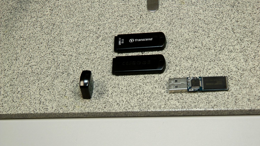
With the help of scalpel, we will open the plastic cover of our USB Flash Drive.
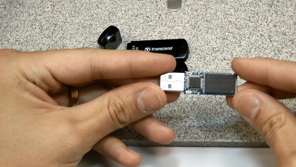
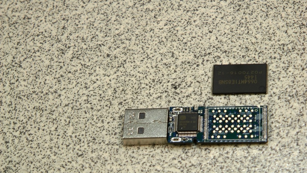
Inside plastic cover, we found a small PCB with SM3257EN controller and one physical chip in TSOP-48 package. We can also found that current PCB has mounting place for two chips – from both side of it. Also, manufacturer prepared interface for two memory chip types – LGA-52 and TSOP-48.
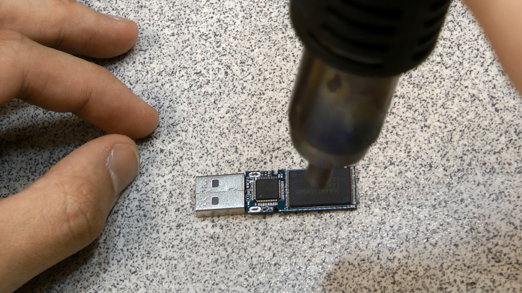
First of all, we need to set our hot air gun to 200C degree, and carefully warm the whole PCB for 10-15 seconds.
We need to warm the whole drive because high temperature difference between cold parts and very hot parts of PCB and chip, might be the reason of additional problems.
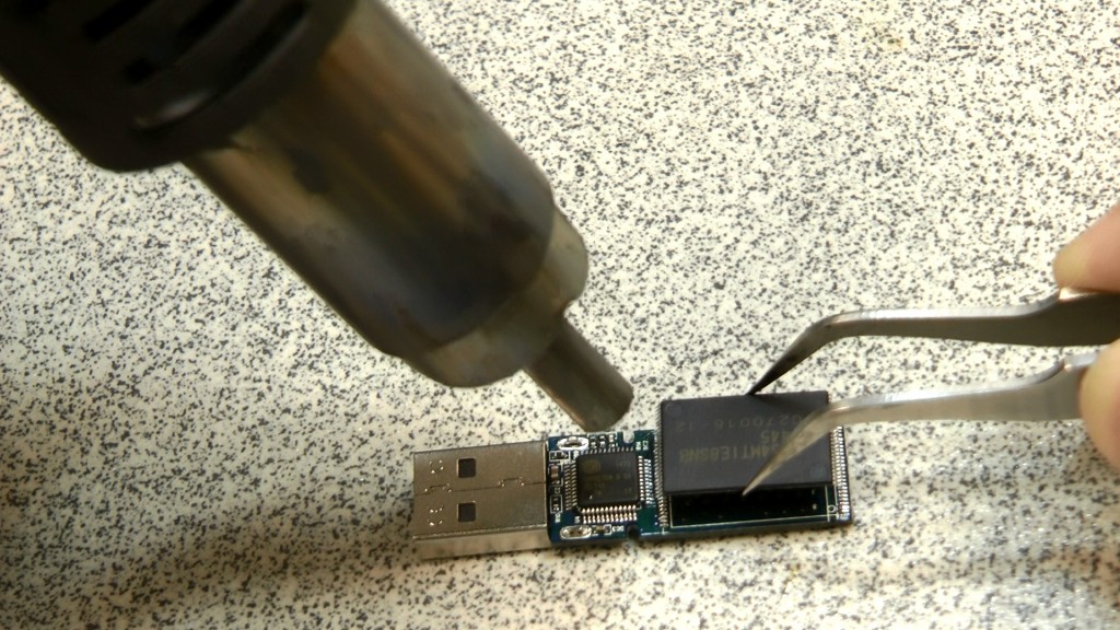
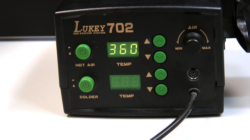
After 15 seconds, lets increase the temperature up to 360C degree. This temperature – is the best compromise between the speed of unsoldering and lower heating influence on the NAND cells.
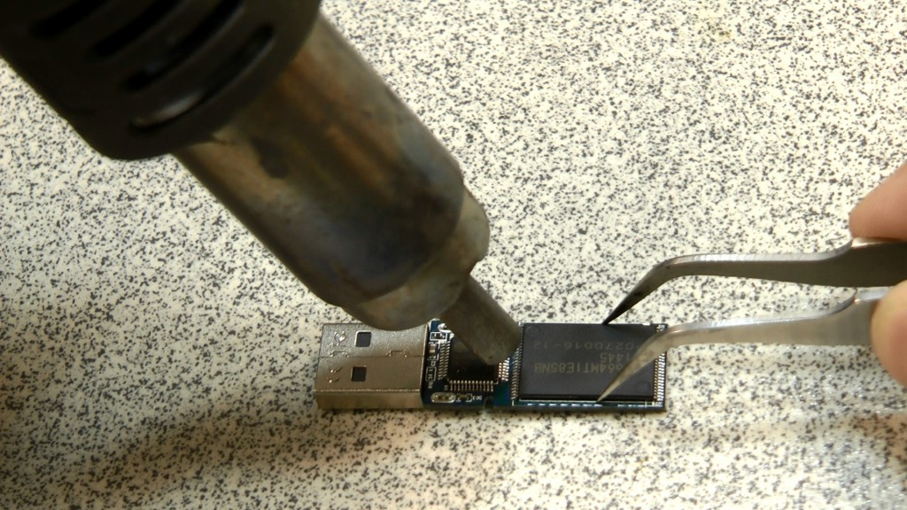
Than – without unnecessary rush, we are keeping to heat the contacts of memory chip – from one side, and from another. Better to hold memory chip in tweezers – it will help us to understand, when the pads on PCB are melt enough for unsoldering.
After approximately 25-40 seconds, chip will be unsoldered. Be careful! Chip is very hot!
Need to wait a couple of minutes, before the chip will not cold down.
The next very important step – is memory chip cleaning.
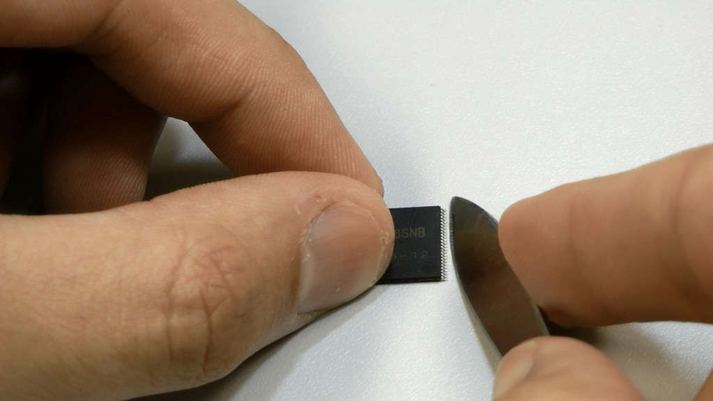
We need to remove the layer of oxid from the upper side of chip contacts. Also, we need to remove all small pieces of solder between the contacts – they can be the reason of wrong chip ID during NAND reading. Make a very careful scratching movement of scalpel along the contacts. Be careful! Do not cut chip legs! After cleaning operation, you can additional clean the chip contacts with isopropyl alcohol.
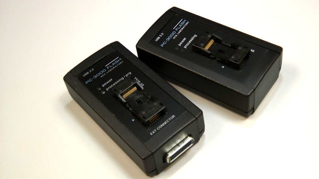
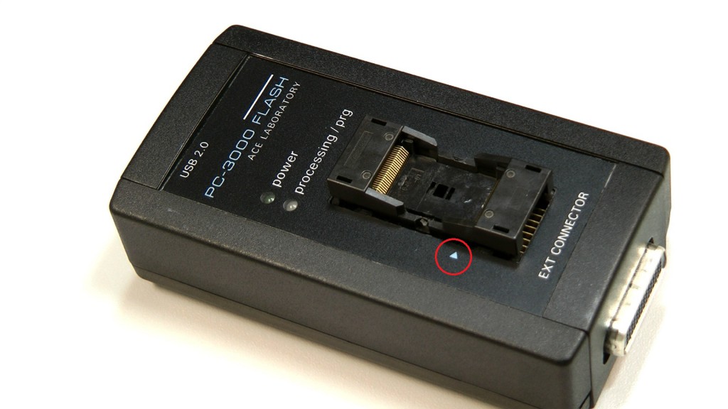
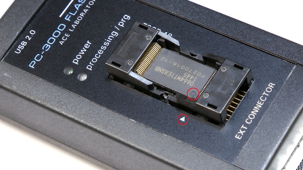
The procedure of chip installation inside PC-3000 Flash reader is the same for all models of Flash reader tools.
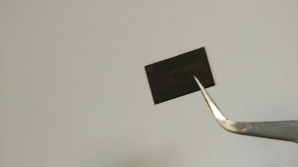
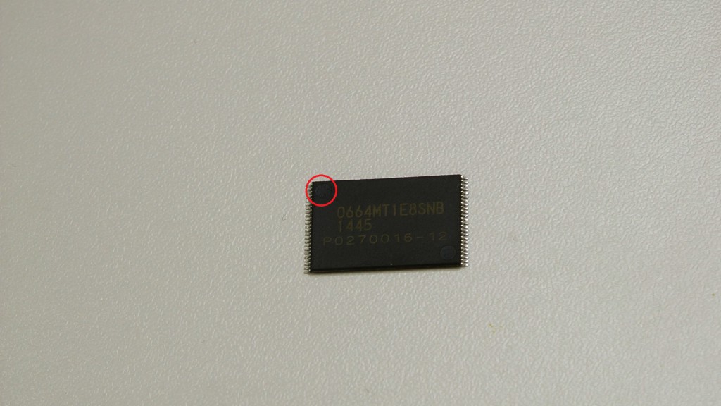
We should replace our memory chip with the following position – blue trangle on reader must be situated near the KEY point on NAND memory chip (the correct KEY point in NAND – is always the point which is situated in the top left corner from the READABLE chip marking!)
That’s all! Now, our chip is ready to be read by PC-3000 Flash.
P.S. About memory chip ID reading you can read here.





respected sir, Kindly respond to my following queries
1. do all the pen drive chips work with this divice,
2. what about android memory is there any dongle to read that mobile chip also
its cost and support.
Regards….. Er. Kamal Dev Panjab India
PC-3000 Flash is support 98% of all ONFI-based NAND chips in the market.
For Android recovery, we have another tool:
http://www.acelaboratory.com/news/newsitem.php?itemid=206